EE 2212
EXPERIMENT 6
2
March 2017
MOSFET I-V Characteristics
Report Due:
16 March 2017
PURPOSE
To measure the I-V
characteristics of an N-channel MOSFET on the CD 4007 array
COMPONENTS
Ø CD4007 MOSFET array
PRELAB
Prepare a detailed circuit
diagrams in your notebook of how you will connect an NMOS for measuring the I-V
curves and how you will connect the inverter circuits. Study the material in Chapter 4. A complete
manufacturer’s data sheet has been posted as a pdf file on the class WEB page.
The device you will use
throughout this experiment and Experiment 7 is a CD4007B Transistor array. It
contains three N-channel and three P-channel devices connected as shown. Detailed schematic diagrams and pinouts are
available on the data sheet and also given below, Figure 6.1. Please use care when working with these
chips. They are very susceptible to excessive voltage and ESD (Electro-Static
Damage). Do not exceed the experiment
settings in an attempt to make your experiment work. The pin
configuration is given in Figure 5.1.
Note that you will be using the CD4007B which have a lower maximum
voltage rating than the CD4007UB. The
diagrams are the same for both the “B” and “UB” suffix devices. Avoid exposing the chip to ESD (electrostatic
damage). This time of the year often has
low relative humidities which make ESD more of an
issue. Do not exceed the VDD
maximums!!!
Study the I-V curves provided in
the data sheets so that you have some idea of what to expect. Also study the chip circuit diagram. You should be able to identify the operation
and function of all of the individual devices.
Observe the input protection circuitry that we will discuss
in Wednesday’s class.
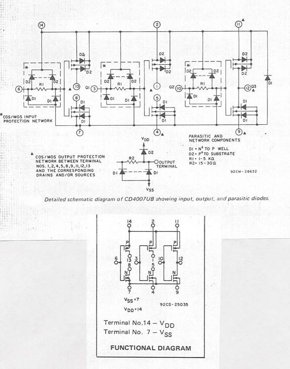
Figure 6.1 Pin Configuration of CD4007.
Warning: Pin 14 should always be connected to the
most positive dc voltage in the circuit.
Pin 7 will always be connected to the most negative dc voltage in the
circuit
(or
else ![MCBS00726_0000[1]](Experiment6MOSI-VCharacteristics_files/image004.gif) )!!!
)!!!
PROCEDURE
I-V Characteristic of an
N-channel MOSFET
Ø Connect the circuit shown in Figure 6.2. Use
the NMOS connected to pins 6, 7, and 8. Remember
to connect pin 14 also to the +VDD supply. Pin 7 is shown connected to
ground. Although you can use the built-in mA meter on the power supply to
measure ID , a better way yielding better accuracy is to measure
current by measuring the voltage drop
across a 100 Ω resistor connected from Pins 8 and 14 and realizing
that ID = V(across the
resistor)/100Ω
Ø Do not use the digital multimeter to measure current because of the hassle in
replacing the internal fuse. Use the
voltage readout on the power supply as you sweep VDD from 0 to 10 volts for each value of VGS from 0 to 6
volts in 1-volt increments. Measure VDS
and ID for each value of VGS using the multimeter. Note that VT is in the 1 to 2 volt
range. Refer to the data sheets where
similar curves are illustrated.
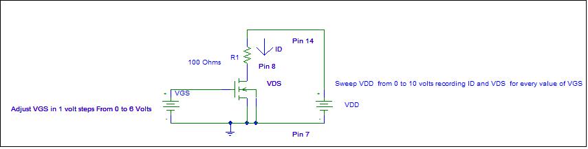
Figure 6.2 ID-VDS As A Function of VGS
Characteristic Measurement For an NMOS
Ø Note that you should keep below ID
= 10mA; since
this is the maximum rated value for this chip, consequently you may not be
able to use all values of VGS depending upon your chip. Plot
data as you proceed.
Ø Using an EXCEL
spread sheet and extracting graphs from the spread sheet is a good way to
display and understand the data.
Ø The CD 4007 is
unforgiving for ESD and over voltage and over current.
Ø Plot your data and use a linear regression
(least squares fit) to extract values for VTO, LAMBDA, and KP and develop a
SPICE model that compares well with your measured curves. An EXCEL spread sheet works well and yields
nice graphs. The objective is to obtain
ID versus VDS for several different values of VGS. Look at Figures 5 and 8 on the CD 4007 data sheet as a guide
as to what to expect. You will have to
assume W/L=1 because you do not know the actual values of W and L and then
adjust KP accordingly. This model
development from your parameter extractions should be included in your report.
Develop a Shichman-Hodges model equation for your NMOS.
Ø Observe that SPICE syntax for Kn’ (for an NMOS) and Kp’ (for
a PMOS) is KP independent
whether you are modeling an NMOS or PMOS.
Refer to Table 4.2 from the text; also on the EE 2212 WEB page. We will do more with notation in Wednesday’s
class.
Now to assist with your
mathematics skills:

How I feel WINDOWS 10 on my DELL
computer.
iOS is much better!

![]()