EE 2212
EXPERIMENT 4
28 February and 7 March 2013
ADDITIONAL DIODE CIRCUITS
This is
a two week experiment. Work to be done
28 February and 7 March
with a report due Thursday, 14 March. The report is to be double length, that is a maximum of 6 pages plus a cover page,
which includes an abstract, in the usual
format. The report will be evaluated on
a 40-point scale, rather than a 20-point scale.
PURPOSE
Experimentally
study the following circuits
Ø Double-diode
clipper; both time domain and transfer (vo versus vs) characteristics
Ø AND Gate
Ø OR Gate
Ø Precision
Rectifier, time domain and transfer characteristics
Ø Obtain Cj(VR) for the 1N4001 by
constructing an adjustable corner frequency analog passive low-pass filter and
compare to the data sheet. This is the
only circuit that requires some computations.
BACKGROUND
In
addition to rectification related to power supply applications as demonstrated
in Experiment 3, diode circuits are used to obtain a variety of important signal processing functions. Among them is the
clipper, precision rectifier, LC network electronic tuning, and diode
logic. You will have an opportunity to
demonstrate these applications both experimentally and using SPICE
simulations.
Ø For example,
inherent in many ICs is the use of diodes to limit input voltage transients to
levels that do not damage the IC. We
will observe this necessary diode protection function when we study MOS and
CMOS IC technology in
a couple of weeks. Virtually all MOS ICs
have this integral to their design.
Ø Diode logic is a
good way to illustrate Boolean functions using simple hardware realizations and
useful for power switching applications.
Refer to your 25 and 27 February class notes on the AND and OR gates implemented with diodes. To a degree, diode logic is part of more
complex digital IC families.
Ø Precision
rectification is used in DSP (Digital Signal Processing) applications where the
“switch” and absolute value function needs to be implemented but there must be
a minimization of the effect of the diode forward voltage. Can we design a circuit that negates the 0.7
volt forward voltage drop? Of course the answer is yes or why would we spend
the time in the lab!
Ø We will also
study “electronic tuning” of a circuit.
We will also measure
Cj(VR) for the 1N4001 by
constructing an adjustable corner frequency analog passive low-pass
filter. The Cj(VR)
is useful for electronic tuning of communications systems. Refer to the 1N4001 data sheet distributed on
the class WEB page as
well as the specialty devices on the Motorola data sheets, also distributed on the class WEB page. Also refer to Problem Set 5. It is important to review the passive LPF
circuits we discussed in class and measured in lab the first two weeks of the
semester.
COMPONENTS
Ø 1N4001 silicon
diodes
Ø mA741 operational amplifiers
Ø A selection of
resistors between 1 kW and 100 kW
PROCEDURE
Ø Construct the
circuit shown in Figure 1. This circuit
is called a Double-Diode Clipper.
Initially, set vs(t) = 7 sin (2p x 100t). Slowly adjust the amplitude of vs(t)
and observe and record the effect on vo(t)
for various positive and negative values of V1 and V2. Also look at the transfer characteristics
and compare your results to the handout distributed in class. A triangular wave with a 7
volt peak amplitude will also work.
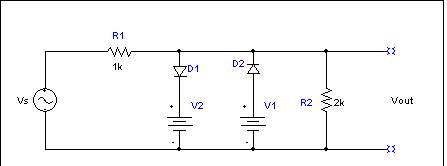
Figure 1 Double-Diode Clipper
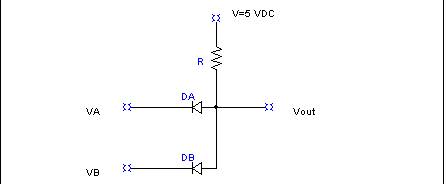
Ø Construct the
circuits shown in Figures 2 and 3 , an AND gate and OR
gate respectively. Set various
combinations of VA and VB voltage levels to verify the appropriate logic gate
operation. Use a square wave on one of the inputs
recognizing that you will need to DC off set the square wave voltage such that
the minimum voltage is 0. Suggest R on
the order of 5 kW.
Define the voltage ranges for the
LOGIC ZERO and ONE logic levels
 .
.
Figure 2 Diode Logic AND Gate
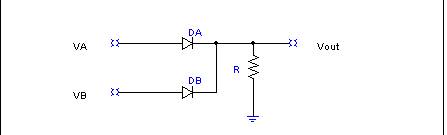
Figure 3 Diode Logic OR Gate
Ø Measure the
transfer characteristic of the circuit shown in Figure 4a. Pay particular attention to the effect of the
diode offset voltage. Now construct the
circuit shown in Figure 4b. Use ±12 volts for the mA 741 operational amplifier. Measure the transfer characteristic and
compare to the results in Figure 4b.
Justify the term “precision rectification” when applied to the circuit
in Figure 4b. Refer to Section 12.8 of
the text, page 760.
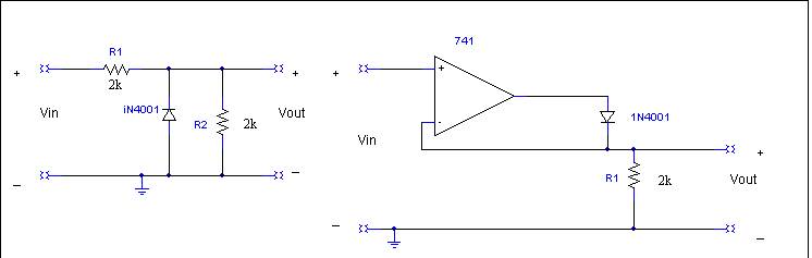
Figure 4(a) Figure
4(b)
Ø This portion of
the experiment will allow you to measure
Cj(VR) for the 1N4001 by
constructing an adjustable corner frequency analog passive low-pass filter
. These measured results will then be
compared to the data curves distributed on the class WEB page and a SPICE
simulation. Construct the circuit shown
Figure 5(a). You will need to determine
the effective value of R2 and CFixed. The
best approach for determining R2, which is the input resistance of the oscilloscope is by using a DC voltage divider with R1. It
will either be 1 Megohm or 10 Megohms
depending upon the input resistance of your oscilloscope. It should be marked near the oscilloscope input
connectors. Observe that the signal
generator allows you to include a DC offset.
The best approach to determine CFixed which includes the
effective capacitance of your leads, the oscilloscope, and the terminal strip
with your wiring is by measuring the -3 dB corner frequency and back
calculating to obtain a value for CFixed. Basically, sweep the frequency of Vs with VDC
= 0 to obtain the basic low-pass filter dB amplitude plot. Now connect the two 1N4001 diodes in the
circuit as shown in Figure 5(b).
Starting with VDC=0, measure the resultant -3 dB corner frequency and
back calculate to obtain Cj for the 1N4001. Recognize that you must subtract the CFixed and there are two diodes in
parallel. We assume both diodes are
identical and the reason two diodes are used is to improve accuracy within the
ranges of our instruments. Continue with
several other values of VDC so that you have several values of Cj to compare with the 1N4001 data curves and to
generate a CJO for a SPICE simulation.
You will also
compare against the SPICE 1N4002 library model. Also note that a data sheet for CJ for the
1N4XXX diode family was distributed on the class WEB page. To minimize the value of CFixed , be neat with your wiring dress. Also note that the scope cables will add about 30 pF/foot.
Check this using the capacitance meter.
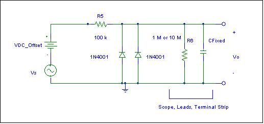
Figure 5(a) Baseline Circuit
Figure
5(b) Diode Capacitance Measurement
Circuit, Tunable Low-Pass Passive Filter
For
all the circuits, compare your experimental results with SPICE simulations and
support your discussions from circuit analysis.
Use the .TRAN SPICE analysis for the first four circuits and the AC
analysis for Circuit 5.
TO THINK ABOUT AND INCORPORATE IN YOUR
REPORT
Ø Did the circuits
operate as expected? Justify
analytically and using SPICE.
Ø How did the diode
offset voltage effect the results?
Ø Suggest system
applications for all the circuits.
This a historically classic data sheet for a
Write Only Memory produced by Signetics
Engineers with too much time on their
hands. It actually slipped by the Signetics QC managers
and was published in a data book before the “joke” was discovered. It has become a classic in the semiconductor
industry. Read it carefully and enjoy!