EE 2212
EXPERIMENT 7
19 November and 3 December 2015
BJT CURRENT SOURCE AND THE EMITTER-COUPLED
PAIR
Note 1: No report is required, however all work and comments should be in your notebook. I will individually review your notebook in the
lab, 10 December. If some of want to
move your review from the afternoon to the morning session, that would help.
Note 2: The CA 3046 is the same electrically as the
LM 3046. Just a different manufacturer.
PURPOSE
The purpose of this experiment
is to characterize the
properties of a:
Ø Basic/Simple Current Source
Ø Emitter-Coupled Pair
COMPONENTS
Ø LM3046/CA3046 transistor array. The data sheet is posted on the class WEB
page
Ø Resistors and potentiometers as required
for the current sources.
Ø 20 kΩ resistors matched as best as
possible.
PRELAB
Compute the values of the
resistors you will need to evaluate the simple current source at the indicated
current level. Also compute resistor and
Q-point values for the emitter-coupled pair.
GENERAL INFORMATION
Ø In IC biasing networks, it is essential
that transistors be well matched and parameter variations track with
temperature. Figure 1 is a pin-out of
the LM3046/CA3046 Transistor Array. Observe that you MUST connect Pin 13, the
IC substrate, to
the most negative point in the circuit or bad things happen to the IC and the
resultant fragrance in the lab is unmistakable.
Ø The only reason there is a fixed 10 kW resistor in the circuit is to protect the
BJT against inadvertent application of a high voltage across the Base-Emitter
junction as you adjust the potentiometer.
You do not want to apply 15 volts to the base of Q1 because the chip
becomes toast (literally and figuratively)!!! Again, bad things happen to the IC and the
resultant fragrance in the lab is unmistakable.
Effectively, the series combination of the 10 kW resistor and the potentiometer is the RREF.
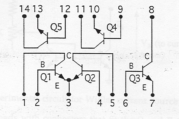
Figure 1 LM3046/CA3046 NPN BJT
ARRAY
SIMPLE CURRENT SOURCE
Figure 2 is a schematic diagram
of a simple current source.
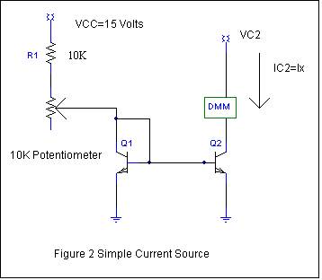
Connect the collector of Q2,
(VC2) to a 5-volt DC supply. Place a DMM
in series with the Q2 collector lead to measure current. If the internal fuse in your DMM is open, replace the DMM with a 1kΩ resistor and
measure the voltage across the resistor and use your results to compute the
current. Same approach as we have done
before. Set IC2=IX to 1 mA by adjusting
the 10 kΩ potentiometer. Compare this value to the reference
current. Measure all key currents and
voltages. Construct the I-V output characteristic by changing VC2 from 0 to 5
volts. Obtain the output resistance
from the slope. Compare to a SPICE simulation to which you have added a finite Early voltage.
EMITTER-COUPLED PAIR
Use Figure 1 and class notes for guidance to
prepare a detailed circuit diagram. We
will cover the emitter-coupled pair starting this Friday. Include pinouts for the LM3046/CA3046 npn
array. From your circuit diagram and circuit specifications, calculate the
expected important Q-point values and Adm .
DC MEASUREMENTS
Refer to the diagram and data
sheet of the LM 3046/CA3046 BJT array.
Set up the circuit in Figure 3 using Q1 and Q2 for
the emitter-coupled pair. Select a value
for REE such that the DC values for Vo1 and Vo2 are about 5 volts. Ground both the inputs of Q1 and Q2.
Measure the all Q-point voltages and currents using the DMM. Use the oscilloscope to also check for
excessive noise which may translate as a noisy dc voltage measurement. Pay particular attention to VOD.
Since the transistors and resistors are reasonably well matched, you would
expect VOD = 0 or reasonably close. If VOD is larger than
a few tens of mV, check your circuit and/or match the collector resistors
better. Lead dress and length is also
important. Be neat! Compare your Q-point values with the expected
and PSPICE simulations. In addition to
using the DMM, look for excessive noise using the scope even though you are
measuring a dc voltage.
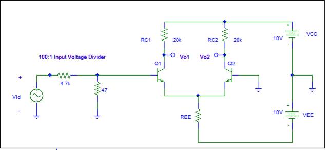
Figure 3
DIFFERENTIAL-MODE OPERATION
Set up your input signals, use
1 kHz, so that the output is reasonably linear. You will need some level of
voltage division as shown in Figure 3.
Figure 3
illustrates a 100:1 divider but the actual divider value is not
critical. Use the oscilloscope and DMM
to measure the differential-mode voltage gain. Compare your results to your
calculations and a SPICE simulation. Include the effect of
a non-infinite Early voltage to improve your analysis and simulation accuracy.
TRANSFER CHARACTERISTICS
The transfer characteristics of
a circuit can be displayed using the X-Y oscilloscope inputs. The amplitude of
the input must be large enough to drive the input through the entire desired
range of operation. You are particularly interested in the VOD
versus VID characteristic. Use a low frequency sinusoid or triangular
wave as the input. From a practical viewpoint, if the input signals are noisy
because of low amplitudes, you will choose to use an input voltage divider to
provide "cleaner" waveforms. Note the 100:1
voltage divider input drive circuit shown in Figure 2, although it doesn’t have to be 100:1. The signal generators have a 100 mV
minimum. By using a 100:1 external
divider, you can achieve a relatively noise free signal at the input to the BJT
bases. Keep track of the divider ratio
you finally use to scale your measurement correctly. Also observe that because
the oscilloscope does not have a floating input (i.e., one side of each of the
two oscilloscope inputs are
connected to ground), you will have to measure either VO1 or
VO2 and scale the final results accordingly by a factor of 2 and
also do not forget the sign (180°phase) differences for each of the outputs.
Show that the slope of the
transfer characteristic will be equal to |Adm/2|.
Compare your results to a SPICE simulation.
Not quite a TESLA but getting
there

After All, This A Lab. How many of you have seen the cute cat
videos?

It is the end of the semester and there are lots of
meetings; some of minimal utility.
Those of you with internships will learn to
appreciate the following: