EE 2212
EXPERIMENT 5
22
October and 5 November
MOSFET I-V Characteristics and MOSFET Circuits

Note 1: Because of the
inter-related nature of the MOS topics, this laboratory set of experiments will
extend over two weeks. Recall that
there is no laboratory on 29 October, Fall Recess.

(May be a bit early for this but Thanksgiving recess is coming in a
month!)
Note 2: The report will be due on 12 November and will be valued at 40 Points. All
rubric values will be multiplied by two compared to the 20 Point rubric.
Note 3: There is a six (6) page limit exclusive of the cover page.
Note 4: You will have enough
class backround through this Wednesday’s class to
proceed through the NMOS resistively-loaded amplifier circuit.
Note 5: There is a noon
seminar by Bruce Howell, Cirrus Design, which means that I will only be in the
lab until 11; Karin will assist at noon.
I am arranging the lab work such that the morning lab can complete the
work during the second week.
PURPOSE
1. To measure
the I-V characteristics of an N-channel MOSFET on the CD 4007 array
2. Measure and simulate the transfer
characteristics (input/output
characteristics) of:
Ø NMOS Inverter with a Resistive Load
Ø NMOS Inverter with an Active Load
Ø CMOS Inverter
Ø CMOS Inverter effective output (Thevanin) resistance.
COMPONENTS
Ø CD4007 MOSFET array
Ø 0.01mF capacitor
Ø 3.3 kW and 100 W resistors
PRELAB
Prepare a detailed circuit
diagrams in your notebook of how you will connect an NMOS for measuring the I-V
curves and how you will connect the inverter circuits. Study the material in Chapter 4. A complete
manufacturer’s data sheet has been posted as a pdf file on the class WEB page.
The device you will use
throughout this experiment is a CD4007B Transistor array. It contains three
N-channel and three P-channel devices connected as shown. Detailed schematic diagrams and pinouts are
available on the data sheet and also given below. Please use care when working with these
chips. They are very susceptible to excessive voltage and ESD (Electro-Static
Damage). Do not exceed the experiment
settings in an attempt to make your experiment work. The pin
configuration is given in Figure 5.1.
Note that you will be using the CD4007B which have a lower maximum
voltage rating than the CD4007UB. The
diagrams are the same for both the “B” and “UB” suffix devices. Avoid exposing the chip to ESD (electrostatic
damage). This time of the year often has
low relative humidities which make ESD more of an
issue. Do not exceed the VDD
maximums!!!
Study the I-V curves provided in
the data sheets so that you have some idea of what to expect. Also study the chip circuit diagram. You should be able to identify the operation
and function of all of the individual devices.
Observe the input protection circuitry that we discussed in last Friday’s
class.
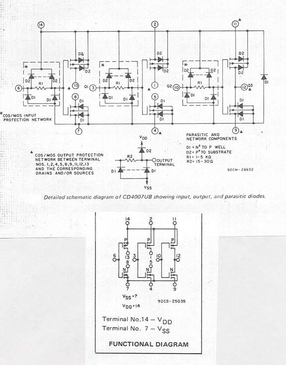
Figure 5.1 Pin Configuration of CD4007.
Warning: Pin 14 should always be connected to the
most positive dc voltage in the circuit.
Pin 7 will always be connected to the most negative dc voltage in the
circuit
(or
else ![MCBS00726_0000[1]](Experiment5MOS_files/image007.gif) )!!!
)!!!
PROCEDURE
I-V Characteristic of an
N-channel MOSFET
Ø Connect the circuit shown in Figure 5.2. Use
the NMOS connected to pins 6, 7, and 8 and 14.
Remember to connect pin 14 also to the +VDS supply. Pin 7 is shown
connected to ground. Use the built-in mA
meter on the power supply to measure ID . I discourage use of the digital multimeter to measure current because of the hassle in
replacing the internal fuse. Use the
voltage readout on the power supply as you sweep VDD from 0 to 10 volts for each value of VGS from 0 to 6
volts in 1-volt increments. Note that VT
is in the 1 to 2 volt range. Refer
to the data sheets where similar curves are illustrated.
Ø Another approach to measure current is to
measure the voltage drop across a 100 Ω resistor connected from Pins 8 and
14.
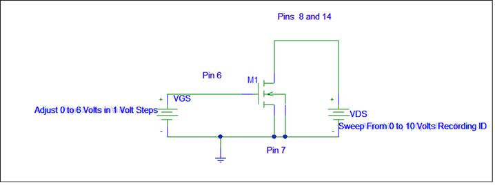
Figure 5.2 ID-VDS As A Function of VGS
Characteristic Measurement For an NMOS
Ø Note that you should keep below ID
= 10mA; since
this is the maximum rated value for this chip, consequently you may not be
able to use all values of VGS depending upon your chip. Plot
data as you proceed.
Ø Using a spread sheet
and extracting graphs from the spread sheet is a good way to display and
understand the data.
Ø The CD 4007 is
unforgiving for ESD and over voltage and over current.
Ø Plot your data and use a linear regression
(least squares fit) to extract values for VTO, LAMBDA, and KP and develop a
SPICE model that compares well with your measured curves. The objective is to obtain ID versus
VDS for several different values of VGS. Look at Figures 5 and 8 on the CD 4007 data sheet as a guide
as to what to expect. You will have to
assume W/L=1 because you do not know the actual values of W and L and then
adjust KP accordingly. This model
development from your parameter extractions should be included in your report.
Develop a Shichman-Hodges model equation for your NMOS.
Ø Observe that SPICE syntax for Kn’
(for an NMOS) and Kp’ (for
a PMOS) is KP independent
whether you are modeling an NMOS or PMOS.
Refer to Table 4.2 from the text; also on the EE 2212 WEB page.
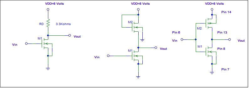
INVERTER CIRCUITS
Refer to the three circuit
diagrams in Figures 5.3, 5.4, and 5.5. All will operate with a VDD = +8 volt
power supply. Remember Pin 14 should
always be connected to the most positive dc voltage in the circuit. Pin 7 will always be connected to the most
negative dc voltage in the circuit.
You will need to arrange for an
offset voltage from the signal generator so that Vin
does not go below zero volts.
To standardize on the SPICE
simulations, use VTO = 2 volts for the NMOS and -2 volts for the PMOS; λ=
0.02 volts-1, and KP = 50E-3.
The default KP does not have enough gain. Use default values for all
other SPICE model parameters.
1. Set up the NMOS Inverter with a Resistive
Load as shown in Figure 5.3. Use the NMOS FET connected to Pins 6, 7, and
8. Plot the transfer characteristic.
Identify the saturation, ohmic, and cutoff regions of
operation. Connect the input and output to the horizontal and vertical inputs
(respectively) of your oscilloscope set to the x-y mode. This arrangement allows
you to display the transfer characteristic of the circuit. Suggest a Q-point to obtain the largest
small-signal voltage gain. Verify your experimental results with a load line
and SPICE simulation. You will need your model parameters as obtained earlier
in this experiment. Observe that you
will need to provide a dc offset from the signal generator.
2. Set up the actively-loaded NMOS Inverter as
shown in Figure 5.4. Use M1 Pins 6, 7,
and 8 and M2 Pins 3, 4, and 5. Connect
the input and output to the horizontal and vertical inputs (respectively) of
your oscilloscope set to the x-y mode. This arrangement allows you to display
the transfer characteristic of the circuit.
Plot the transfer characteristic. Identify the saturation, ohmic, and cutoff regions of operation for each FET.
Suggest a Q-point to obtain the largest small-signal voltage gain. Verify your
experimental results with a “load line” which consists of the M2 characteristic
and SPICE simulation. Compare your results with the resistively-loaded circuit.
Note that this circuit is different than the depletion mode inverter circuit discussed and SPICE
demonstrated in class. Observe that you will need to provide a dc
offset from the signal generator.
![]()
Figure 5.3 NMOS Inverter Resistive Load Figure 5.4 NMOS Inverter Active Load Figure 5.5 CMOS Inverter
3.
Connect the CMOS inverter circuit of Figure
5.5. with the pins shown. You can also use the CMOS inverter FETS
connected using Pins 9, 10, 11, and 12.
Connect the input and output to the horizontal and vertical inputs
(respectively) of your oscilloscope set to the x-y mode. This arrangement
allows you to display the transfer characteristic of the circuit. Before
connecting your function generator to the circuit input, adjust it for a 0-8 V
triangular waveform at a frequency of 1 kHz. You will need to use the dc-offset
control on your function generator to do this. That is an 8 volt peak-to-peak
triangular wave added to a 4 volt dc offset.
Observe and sketch the transfer characteristic, recording all critical
values of voltage. Your report should
include a PSPICE simulation of this circuit using your parameter extraction
NMOS and PMOS models. Compare to the
4007 curves on the
data sheets.
4.
Refer
to Figure 5.6. Measure the pulse
response of the CMOS inverter with a capacitor Co that has been
added from the output to ground to “slow down” the output waveform so that
measurements can be more easily made. Since the input of a CMOS gate is
primarily capacitive, this also will provide the output behavior when a CMOS
gate is driving many other CMOS gates (a capacitive load). Adjust your function
generator to 0 to 8V square wave at a frequency of about 10 kHz, then connect
it to the input. Measure the rise and fall times of Vout(t). You
should be able to compute the effective value of the CMOS inverter output
resistance, Req, from the rise and fall
time measurements. Refer to what you did
in Experiment 1 for a basic RC network.
Compare your measured results with a PSPICE simulation.

A few more items to think about.
Compare the static power dissipation of the four circuits CMOS Inverter, NMOS
Inverter with a resistive load, NMOS inverter with an active load, and the NMOS
NOR gate with a resistive load) when operated as switches/inverters as opposed
to amplifier operation.
Now to assist with your
mathematics skills:
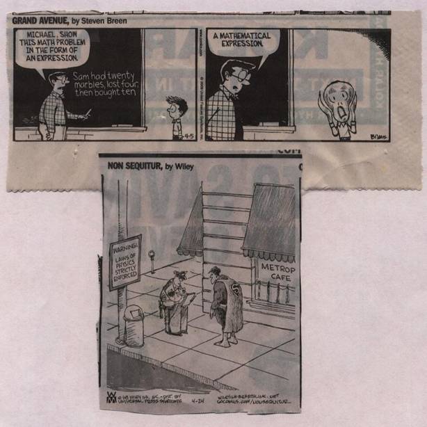

How I feel about some aspects of
WINDOWS 8 and now WINDOWS 10 is coming!

![]()