EE 2212
EXPERIMENT 4
15 October 2015
DIODE ODDSAND
ENDS CIRCUIT APPLICATIONS
20 Point Rubric
Report Due: 22
October
Note:
This is a relatively short lab which shouldn’t take more than an hour or
so. Since I have a visitor from GeaCom, I will have to leave about 11. Karin Larson will stop by at noon if you are
still working on the lab and need some additional guidance. I would like everyone to be able to attend
the noon GeaCom seminar. No time conflicts with the afternoon lab
although I may be a few minutes late.
PURPOSE
Experimentally study the
following circuits
Ø Double-diode clipper; both time domain and
transfer (vo versus vs) characteristics
Ø AND Gate
Ø OR Gate
BACKGROUND
In addition to rectification
related to power supply applications as demonstrated in Experiment 3, diode
circuits are used to obtain a variety of important signal
processing functions. Among them
is the clipper and diode logic You will have an opportunity to demonstrate
these applications both experimentally and using SPICE simulations.
Ø For example, inherent in many ICs is the
use of diodes to limit input voltage transients to levels that do not damage
the IC. We will observe this necessary
diode protection function when we study MOS and CMOS IC technology starting next week. Virtually all MOS ICs have this integral to
their design. This is also the concept
of the surge protector you have for your delicate electronic stuff.
Ø Diode logic is a good way to illustrate
Boolean functions using simple hardware realizations and useful for power
switching applications. Refer class
notes on the AND and OR gates implemented with
diodes. To a degree, diode logic is
often the basis
underlying complex digital IC families.
COMPONENTS
Ø 1N4001 silicon diodes
Ø 1, 2, and 5 kW resistors (approximate values)
PROCEDURE
Ø Double-Diode Clipper
Construct
the circuit shown in Figure 1. This
circuit is called a Double-Diode Clipper.
Initially, set vs(t) = 5 sin (2p x 100t). A triangular wave with a 5 volt
peak amplitude will also work. Slowly adjust the amplitude of vs(t) and observe and record the effect on vo(t) for various positive and negative
values of V1 and V2. Also look at the
transfer characteristics. You will need
to switch the polarity and magnitudes of V1 and V2 (4 permutations of polarity)
to note the clipping effects under all voltage polarity and amplitude
conditions. To a large extent, your data
collection will be qualitative. Transfer
characteristics, that is vo(t) versus vs(t),
is an excellent way to display your results. This
circuit concept is
integral to most MOSFET ICs to protect against ESD (Electrostatic Damage). We will talk more about ESD next week.
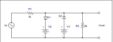
Figure 1 Double-Diode Clipper
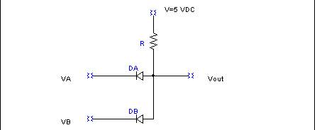
Ø Diode Logic Gates
Construct
the circuits shown in Figures 2 and 3 , an AND gate
and OR gate respectively. Set various
combinations of VA and VB voltage levels to verify the appropriate logic gate
operation. Use a square wave on one of the inputs
recognizing that you will need to DC offset the square wave voltage such that
the minimum voltage is 0. The other
input can be a zero volt or 5 volt input from your power supply. Suggest using an R pull-up and pull-down resistor on
the order of 5 kW. Define the voltage ranges for the LOGIC ZERO and ONE logic
levels. Refer to DiodeGates.docx on the class WEB page.
 .
.
Figure
2 Diode Logic AND Gate
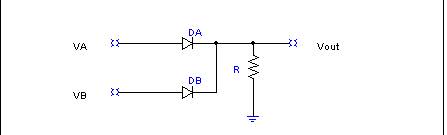
Figure
3 Diode Logic OR Gate
TO THINK ABOUT AND INCORPORATE
IN YOUR REPORT
Ø Did the circuits operate as expected? Justify analytically and using SPICE.
Ø How did the diode offset voltage effect the
results?
Ø Suggest system applications for all the
circuits.
When
you go home for Fall Break, Thanksgiving, and Winter Recess, you should be
prepared to do the following: (Also for
Smart Phones, etc,)

I just received notification
about Spring class registration that is coming up
soon. Some of you may choose to work on
an Energy Engineering Minor.