ECE 2212
EXPERIMENT 5
24
October 2013
MOSFET I-V Characteristics and MOSFET Circuits
PURPOSE
To measure the I-V
characteristics of an N-channel MOSFET and a P-channel MOSFET on the CD 4007 array.
PRELAB
Prepare a detailed circuit
diagram in your notebook of how you will connect an NMOS and PMOS for measuring
the I-V curves. Study the material in
Chapter 4. A complete manufacturer’s data sheet has been posted on the class
WEB page.
The device you will use
throughout this experiment is a CD4007B Transistor array. It contains three
N-channel and three P-channel devices.
Detailed schematic diagrams and pinouts are
available on the data sheet and also give below. Please use care when working with these
chips. They are very susceptible to excessive voltage and ESD (Electro-Static
Damage). Do not exceed the experiment
settings in an attempt to make your experiment work. The pin
configuration is given in Figure 5.1.
Note that you will be using the CD4007B which have a lower maximum
voltage rating than the CD4007UB. The
diagrams are the same for both the “B” and “UB” suffix devices. Avoid exposing the chip to ESD (electrostatic
damage). This time of the year often has
low relative humidities which make ESD more of an
issue. Do not exceed the VDD
maximums!!!
Study the I-V curves provided in
the data sheets so that you have some idea of what to expect. Also study the chip circuit diagram. You should be able to identify the operation
and function of all of the individual devices.
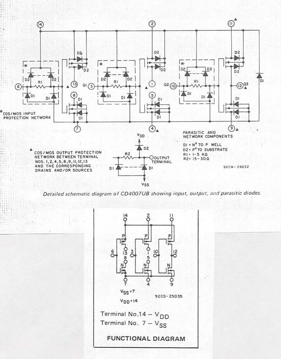
Figure 5.1 Pin Configuration of CD4007.
Warning: Pin 14 should always be connected to the
most positive dc voltage in the circuit.
Pin 7 will always be connected to the most negative dc voltage in the
circuit
(or
else ![MCBS00726_0000[1]](Experiment5MOS_files/image004.gif) )!!!
)!!!
PROCEDURE
I-V Characteristic of an
N-channel MOSFET
Ø Connect the circuit shown in Figure 5.2. Use
the NMOS connected to pins 6, 7, and 8 and 14.
Remember to connect pin 14 also to the +VDS supply. Pin 7 is shown
connected to ground. Use the built-in mA
meter on the power supply to measure ID. Use the voltage readout on the power supply
as you sweep VDD
from 0 to 10 volts for each value of VGS
from 0 to 6 volts in 1-volt increments.
Note that VT is in the 1 to 2 volt range. Refer to the data sheets.
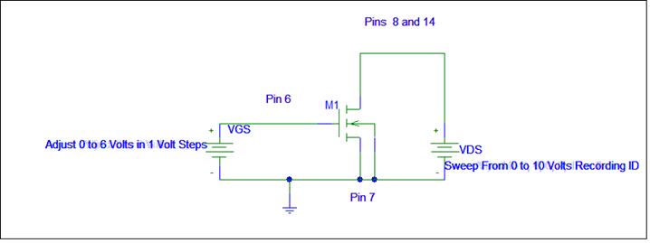
Figure 5.2 ID-VDS As A Function of VGS Characteristic
Measurement For an NMOS
Ø Note that you should keep below ID
= 10mA; since this
is the maximum rated value for this chip, consequently you may not be able
to use all values of VGS depending upon your chip. Plot
data as you proceed.
Ø Plot your data and use a linear regression
(least squares fit) to extract values for VTO, LAMBDA, and KP and develop a
SPICE model that compares well with your measured curves. The objective is to obtain ID versus
VDS for several different values of VGS. Look at Figures 5 and 8 on the CD 4007 data sheet as a guide
as to what to expect. You will have to
assume W/L=1 because you do not know the actual values of W and L and then
adjust KP accordingly. This model
development from your parameter extractions should be included in your report.
Develop a Shichman-Hodges model equation for your NMOS.
I-V Characteristic of a
P-channel MOSFET
Ø Connect the circuit shown in Figure 5.3. Use
the PMOS connected to pins 6, 13 and 7, and 14.
Use the built-in mA meter on the power supply to measure ID. Use
the voltage readout on the power supply as you sweep VDD = -VDS from 0 to 10
volts for each value of VGS from 0 to -6 volts in 1-volt increments. Note that VT is in the -1 to -2
volt range. Refer to the data sheets.
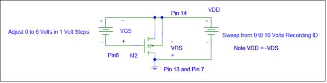
Figure 5.3 ID-VDS As A
Function of VGS Characteristic Measurement For an PMOS
Ø Use the PMOS connected to Pins 6, 13 and 7,
and 14. Note that Pin 13 is the PMOS
drain.
Ø Note that you should keep below |ID| = 10mA; since this is the maximum rated value
for this chip, consequently you may not be able to use all
values of VGS depending upon your chip. Plot
data as you proceed.
Ø Plot your data and use a linear regression
(least squares fit) to extract values for VTO, LAMBDA, and KP and develop a
SPICE model that compares well with your measured curves. The objective is to obtain ID versus
VDS for several different values of VGS. Look at Figures 9 and 10 on the CD 4007 data sheet as a guide
as to what to expect. You will have to
assume W/L=1 because you do not know the actual values of W and L and then
adjust KP accordingly. This model
development from your parameter extractions should be included in your report.
Develop a Shichman-Hodges model equation for your PMOS.
To Assist
with your mathematics skills: