ECE 2212
PROBLEM SET 11
S. G. Burns
Due:
Wednesday, 5 December 2012
Note: You should be able to address Problems 1 and 2 with your knowledge
of small-signal models from the past two weeks of classes. Topics embodied in Problems 3 and 4 were covered
in the Monday, 19 November class.
Problem 5 background will be covered in the Wednesday, 21 November class. The MOS designs and analyses will be covered in the 26 and 28
November classes.
The first two problems are to provide additional
practice in constructing small-signal models
1.
Text 14.1 but only Parts (a), (b), (c), (d),
(g) , (h), and (l). No computations are required. Be sure you carefully label
your small-signal models including all key nodes. Assume capacitive reactances
are very small at the frequency of interest.
2.
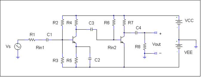
This is a circuit of a two-stage npn-npn cascade amplifier operating between two power
supplies, VCC and a -VEE. Assume that for BJTs Q1 and Q2,
IC1 = 1 mA and IC2 = 2 mA, b1 = 100 and b2 = 150, and both Early voltages are 75 volts.
(a) Draw and label a small-signal, frequency-independent, model. By
frequency-independent I mean that the you should assume capacitive reactances
are very small at the frequency of interest.
(b) Using your small-signal model, derive an algebraic equation for
the voltage gain defined by Av
= Vout/Vs.
(c)
Compute
numerical values for gm, ro,
and rp
for both the npn BJTs.
(d)
Using your small-signal model, derive an
algebraic expression for the input resistance Rin1 and Rin2.
Q2 Q1
![]()
![]()

Study selected portions of text Sections 16.2 through 16.5 related to basic and Widlar BJT Current Mirrors and MOS-based current sources as
well as the class discussions we started on Monday, 19 November.
3. Simple
and Widlar Current Sink and Source Calculations
(a)
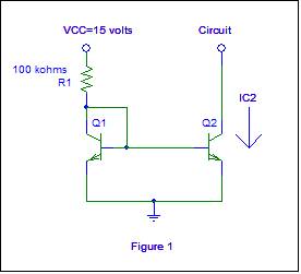
Compute a value for IC2 which is the current you
would sink from a circuit requiring that current bias level.
(b)
Design a pnp circuit based upon the
npn circuit shown in Figure 1 that would operate as a
current source, rather than a current sink,
for the current computed in Part (a).
Your design must include a well-labeled circuit diagram.
(c)
Design a Widlar current source to
sink the current computed in Part (a).
Refer to Figure 2. You have a fair
amount of flexibility in R1 and R2.
Follow guidelines presented in Monday’s , 19
November, class discussion.


4. Combine
the ideas from Problem 3 to design a current source/sink mirror system that
provides 0.5 mA, 1.0 mA,
and 50 μA as shown in the diagram below. The idea is that your circuit design can
directly replace the three current source symbols shown in the diagram.
(a)
You are to use only one reference resistor.
(b)
You will need to use npn
and pnp transistors.
(c)
Different transistor cross-sectional areas are allowed within
the constraints of IC design and reasonableness.
(d)
Assume β >> 1 for
all transistors.
(e)
Assume room temperature operation.
(f)
You should use both basic and Widlar
configurations as appropriate.
(g)
Your design and analysis must show all relevant design
equations and assumptions.
(h)
Your design must include a detailed and accurately labeled
circuit diagram.

5.
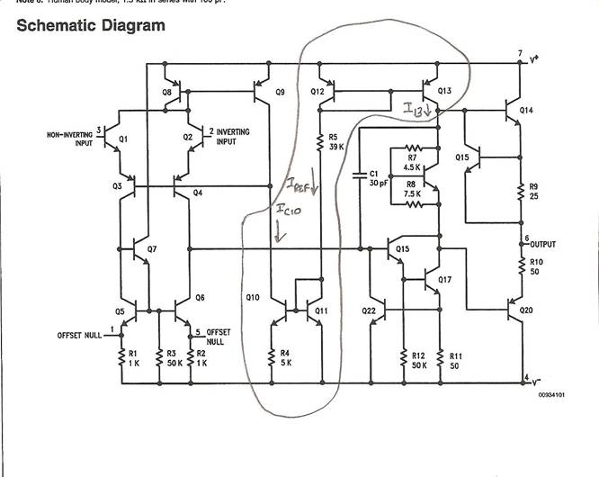
The following is a circuit diagram of a National Semiconductor LM 741
operational amplifier. I have circled
key elements of the current source
system you are analyze. Assume all |VBE(on)| = 0.7 volts. V+ = 12 volts and V- =
-12 volts. All npn transistors have equal junction areas and all pnp transistors have equal junction areas. The Fairchild μA
741 diagram on text page 1097, Figure 16.46, is another variation. I prefer to use the National Semiconductor LM
741 circuit diagram and Signetics μA
741 circuit diagram because they
are a bit easier to read. There are differences in some component
values because they originate from different manufacturers.
Compute
values for IREF, IC10, and I13.

6.
Text 16.8 Parts (b) and (c) only.
Do not do the case for a non-zero λ. This is an NMOS current mirror system.
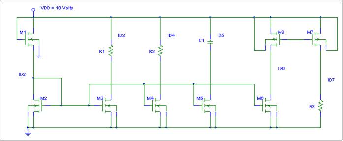
7. MOS Current Mirror System.
Once you realize that ID2 = 50
μA the problem can be done by inspection or at
most, on one line without a calculator! Several elements of this problem were used on
an old quiz.
![]()
![]()
![]()
![]()
![]()
![]()
![]()
![]()

Assume the following:
(a)
M1 and M2 are matched (b)
l = 0 for all MOSFETS (c) L identical for all FETS. (d) ID2 = 50 μA.
(e) W1=W2=W3=W6=W8 (f) W4=W5=2 x W2 (g)
W7 = 3 x W8 (h) Except for W/L
ratios, the fabrication process are the same for all FETs.
Pay attention to sign conventions!
Provide values for:
ID3 =__________________ ID4 = ____________________ ID7
________________
ID5 = _________________ (Trick
question. Careful-look
at the drain circuit for M5!)