EE
2212
PROBLEM
SET 6
S.
G. Burns
Due: Friday, 6 November 2020
1. Figure P4.18
NMOS Characteristics Generate a SPICE
NMOS model by modifying the default NMOS transistor model (MBREAKN in PSPICE ) or
the equivalent in LT SPICE that will reasonably match the curves in P4.18
figure. If you look at the curves, it is
a good assumption that λ = 0. Your
problem submission must include the listing of your modified MOS parameters and
the resultant ID-VDS curves and the SQRT(ID)
versus VGS curve.
2. Figure 4.48
PMOS Characteristics Generate a SPICE PMOS
model by modifying the default PMOS transistor model (MBREAKP in PSPICE ) or
the equivalent in LT SPICE that will reasonably match the curves in P4.48
figure. If you look at the curves, it is
a good assumption that λ = 0. Your problem submission must include the
listing of your modified MOS parameters and the resultant ID-VDS
curves and the SQRT(ID) versus VGS curve.
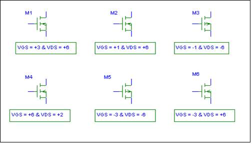
3.
From an old quiz.
Regions of operation are very important in circuit design using
MOSFETS. Extracted from an old
quiz. For the indicated bias conditions, state whether the FET is
operating in the OHMIC (TRIODE) region, SATURATION region, or CUTOFF
region. Explain your reasoning. Assume that |VT | = 2 volts for both the
NMOS and PMOS enhancement mode transistors.
M1 __________ M2
__________ M3 __________
M4
__________ M5 __________ M6 __________
The following problems provide practice in working with
small-signal models. Use the basic voltage-controlled current generator FET
small-signal model with λ (Lambda) =0. In addition to answering the text questions,
you are to draw and label the resultant small-signal model circuit
diagrams. Express your derivations
symbolically; that is no calculations are required. These problems also will familiarize you
with the text FET symbol notation variations.
It is important that you label circuit nodes carefully.
4. Draw the small-signal model for Figure
P13.5. After you have obtained the
small-signal model, derive an equation for the voltage gain defined by av = vo/vi. Observe that
no numerical calculations are
required. Note that this circuit uses an
NMOS. This circuit is a common-source.
5. Draw the small-signal model for Figure
P13.8. After you have obtained the
small-signal model, derive an equation for the voltage gain defined by av
= vo/vi.
Observe that no numerical calculations are required. Note that this circuit uses a PMOS. This circuit is a common-source.
6. Draw the small-signal model for Figure P13.9. After you have obtained the small-signal
model, derive an equation for the voltage gain defined
by av = vo/vi. Observe that no numerical calculations are
required. Note that this circuit uses an
NMOS. The circuit
is a common-gate.
7. Small-Signal
Model derivation for a cascade amplifier
excerpted from an old quiz.
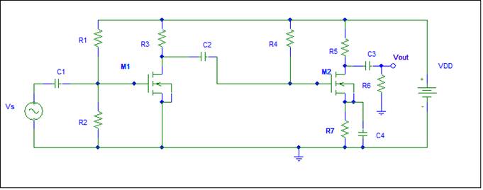
(a) Sketch and label a small-signal model for
this circuit which consists of two Common Source
amplifiers in a cascade configuration.
Assume all capacitors are large at the frequency of interest
. Your model should be complete
and well-labeled.
Assume λ= 0.
(b) Derive an expression for the voltage gain defined by Av = Vout/Vs . Observe no
numerical calculations are required.
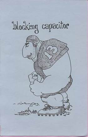
This is what
we use for blocking dc and passing ac in many discrete device amplifier
circuits. Synonymous with coupling
capacitor. Also
a dc blocking capacitor is employed in your oscilloscope when switching to AC
input using the soft keys. Your HANTEK
“CHANNEL” button and Channel selection with allow you switch
coupling by toggling the F3 button.
Consider the signal swing around the Q-Point which established the
dynamic range of a circuit which we will
use in amplifier design

Even though
most of you are EE students, there is some information you can use from CS
I. Of course, you can always dive deeper
into CS but it messy in more ways than one, refer to the figure. I don’t know if this diagram is covered in
more advanced CS courses if you decide to work on a CprE Minor. Can you tell that I am a hardware guy!