EE 2212
PROBLEM SET 10
S. G. Burns
Due:
Wednesday, 20 November 2019
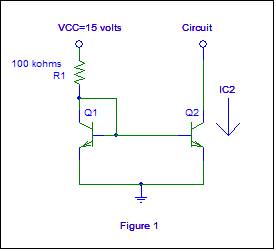
1. Simple
and Widlar Current Sink and Source Calculations
(a)
Compute a value for IC2 which is the
current you would sink from a circuit requiring that current bias level.
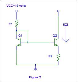
(b)
Design a Widlar current
source to sink the current computed in Part (a). Refer to Figure 2. You have a fair amount of design flexibility
in R1 and the resultant value of R2.
2. Current Source System From
An Old Quiz
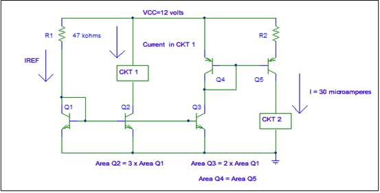
![]()
Assume b >> 1, VBE(on) = 0.7 volts, all npn junction areas identical, and all pnp junction areas are identical.
IREF =
______________ IC2 = _____________________
IC3 =
_______________ IC4 = _______________ R2
= ______________
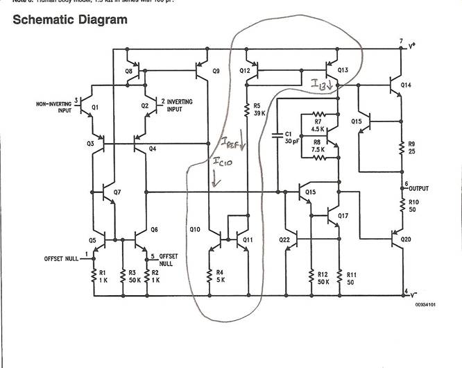
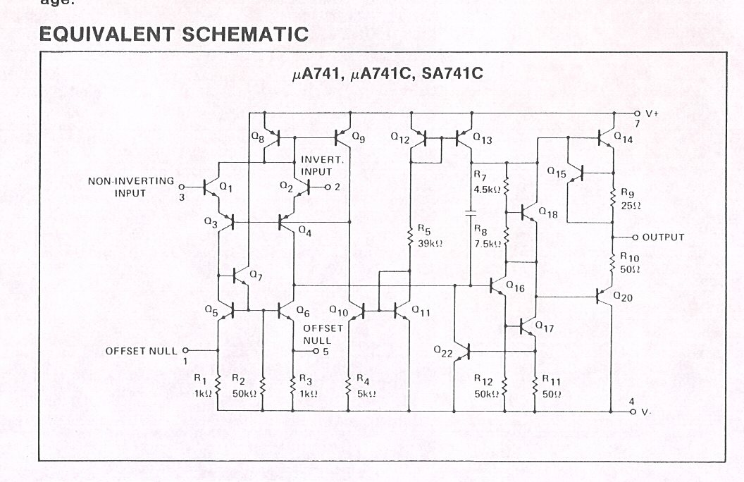
3. The
following is a circuit diagram of a National Semiconductor LM 741 operational
amplifier. Recall from the beginning of the semester that I mentioned that you
will be able to analyze key sub-circuits of operational amplifiers and related
circuits by the end of the semester. I
have circled key elements of the current source system you are analyze in the
LM 741. Assume all |VBE(on)| =
0.7 volts (for both npn and pnp). V+ = 12 volts and V-
= -12 volts. All npn
transistors have equal junction areas and all pnp
transistors have equal junction areas.
741signetics.jpg You will have to
solve a transcendental equation to obtain IC10.
Compute
values for IREF, IC10, and I13.
4.
Text 16.8 Only Part (b) and assume λ = 0. This is an NMOS current mirror system, Figure
16.8. “One liner” of arithmetic without a
calculator”! You can throw away your calculator for this
problem.
5. Adapted from an old
quiz. NMOS Current Mirror System.
Similar to Problem 4 with some added wrinkles.
Once you realize that ID2 = 50 μA the
problem can be done by inspection, or at most on one line, without a
calculator! Several elements of
This problem were used on an old quiz.
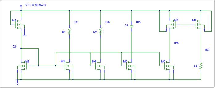
Assume the following:
(a) M1 and M2 are matched (b) l = 0 for all MOSFETS (c) L
identical for all FETS. (d) ID2 = 50 μA.
(e) W1=W2=W3=W6=W8 (f) W4=W5=2
x W2 (g) W7 = 3 x W8 (h) Except for W/L ratios established by the
photolithography design, the fabrication process is the same for all FETs.
Pay attention to sign
conventions!
Provide values for:
ID3 =__________________ ID4 =
____________________ ID7 ________________
ID5 = _________________ (Trick
question. Careful-look at the drain circuit for M5!


