EE 2212
Experiment 7
25 March 2021
MOSFET AMPLIFIER CIRCUITS
Study
time
domain operation and transfer characteristics of two circuits and compare with
the SPICE simulations.
Ø NMOS Inverter with a Resistive Load
Ø CMOS Inverter
COMPONENTS
Ø CD4007 MOSFET array
Ø 9 Volt VDD Battery Pack
Ø 10 K or 100 K potentiometer
Ø 3.3 kW resistor
(Other values will also work)
PRELAB
The device you will use
throughout this experiment is a CD4007B Transistor array. It contains three
N-channel and three P-channel devices connected as shown. Detailed schematic diagrams and pinouts are
available on the data sheet and also given below. Please use care when working with these
chips. They are very susceptible to excessive voltage and ESD (Electro-Static
Damage). Do not exceed the experiment
settings in an attempt to make your experiment work. The pin
configuration is given in Figure 7.1.
Note that you will be using the CD4007B which have a lower maximum
voltage rating than the CD4007UB. The
diagrams are the same for both the “B” and “UB” suffix devices. Avoid exposing the chip to ESD (electrostatic
damage). This time of the year often has
low relative humidity which make ESD
more of an issue.
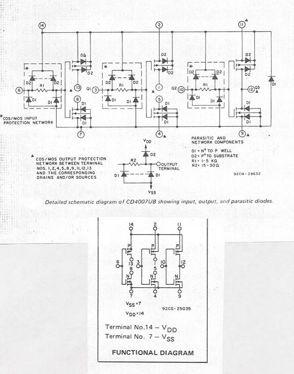
Figure 7.1 Pin Configuration of CD4007.
Warning: Pin 14 should always be connected to the
most positive dc voltage in the circuit.
Pin 7 will always be connected to the most negative dc voltage in the
circuit which is system ground in this case.
(or
else ![MCBS00726_0000[1]](Experiment7MOSAmplifierCircuits_files/image007.gif) )!!!
)!!!
PROCEDURE
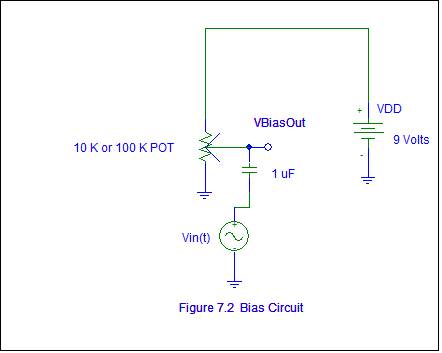
BIAS CIRCUIT
Set up the Figure 7.2 Bias Circuit on your
breadboard. The basic idea is that you
can adjust the dc level from 0 to +9 volts which will be used to bias the
circuits shown in Figures 7.3 and 7.4.
You will then use the
AWG to couple a signal through the 1 uF
capacitor. This input signal will be
shifted to be at the set dc voltage.
·
Set
up the Figure 7.2 circuit on your breadboard.
·
Turn
on the HANTEK and press the AWG button
·
Turn
on the 9-volt power supply
·
Set
the AWG to a 2.5 volt amplitude, zero-volt offset, 1 kHz sine wave. Verify that the Green Icon is lit.
·
Monitor
VBiasOut on Channel 1. Channel Coupling to DC. Use AUTO if necessary
·
Experimentally
adjust the potentiometer and note the dc level shift with the superimposed sine
wave.
·
Set
the dc level to approximately 4.5 volts using the potentiometer
·
Proceed
with this setup to Figure 7.3, NMOS Inverter.
INVERTER CIRCUITS
Refer to the two circuit diagrams in Figures 7.3 and
7.4. All will operate with a VDD = +9 volt power supply. VSS = 0 Volts. Remember Pin 14 should always be connected to
the most positive dc voltage in the circuit.
Pin 7 will always be connected to the most negative dc voltage in the circuit which is
ground for these circuits..
You will need to verify that Vin does
not go below zero volts. With the AWG at
2.5 volts and 4.5 volts of dc bias, the voltage will vary sinusoidally
between 2 and 7 volts.
To standardize on the SPICE
simulations, use VTO = 2 volts for the NMOS and VTO = -2 volts for the PMOS;
λ= 0.02 volts-1, and KP = 50E-3. This works for PSPICE. If you do not have a generic FET in your
version of LT SPICE, then we will have to go through your available library for
FETS that will show the information we need for both circuits. The default KP does not do a good job in
modeling the CD4007 devices which means the circuits will not exhibit the measured
voltage gain. Use default values for all
other SPICE model parameters.
1. Set up the NMOS Inverter with a Resistive
Load as shown in Figure 7.3. Use the NMOS FET connected to CD4007 M1 Pins 6, 7,
and 8.
·
Experimentally
adjust the potentiometer and note the dc level shift with the superimposed sine
wave.
·
Set
the dc level to approximately 4.5 volts using the potentiometer
·
Monitor
the input with Channel 1 and Monitor the output with Channel 2. Compute the voltage gain from these two
waveforms.
·
Adjust
the AWG output to minimize clipping of Vout. Shifting the dc level will also help
centering along the dc load line.
·
Press
the TIME button and toggle F1 to obtain X-Y; that is the Transfer
Characteristic of Vout versus Vin.
·
You
will probably need to carefully adjust the DC bias voltage using the
potentiometer to obtain a complete transfer characteristic. Also look at the time domain Y-T when you
adjust the dc bias voltage level.
![]()
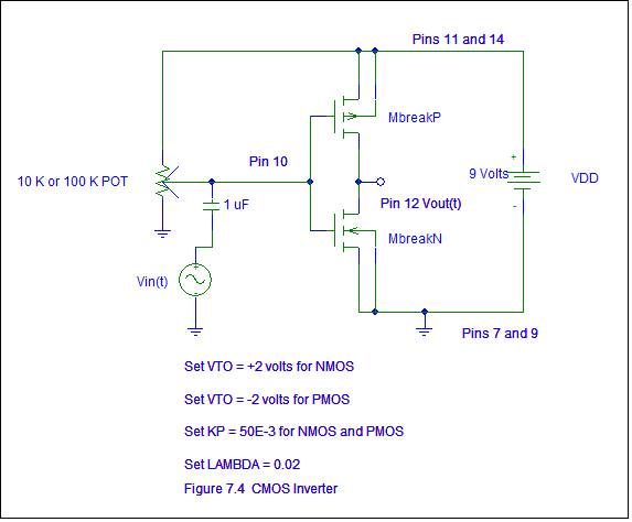
2.
Connect
the CMOS inverter circuit of Figure 7.4. with the
CD4007 pins as shown.
·
Experimentally
adjust the potentiometer and note the dc level shift with the superimposed sine
wave.
·
Set
the dc level to approximately 4.5 volts using the potentiometer
·
Monitor
the input with Channel 1 and Monitor the output with Channel 2. Compute the voltage gain from these two
waveforms.
·
Adjust
the AWG output to minimize clipping of Vout. Shifting the dc level will also help
centering along the dc load line.
·
Press
the TIME button and toggle F1 to obtain X-Y; that is the Transfer
Characteristic of Vout versus Vin.
·
You
will probably need to carefully adjust the DC bias voltage using the
potentiometer to obtain a complete transfer characteristic. Also look at the time domain Y-T when you
adjust the dc bias voltage level.
3.
Your
report should include a PSPICE simulations of both of these circuit using NMOS
and PMOS MBreak and PBreak
models with the values VTO, KP, and LAMBDA included. A few more items to think about. Compare the
static power dissipation of both circuits CMOS Inverter and NMOS
Inverter with a resistive load when operated as switches/inverters as opposed
to amplifier operation.
These Cartoons Represent EE at
its Finest!


![]()