EE 2212
EXPERIMENT 6
11
March 2021
MOSFET I-V Characteristics
PURPOSE
To measure
the VT and k on an
N-channel MOSFET on the CD 4007 NMOS array.
COMPONENTS
Ø CD4007 MOSFET array
Ø Two 9-Volt Battery Supplies
Ø 10KΩ
or 100KΩ Potentiometer
PRELAB
Prepare a detailed circuit
diagrams in your notebook of how you will connect an NMOS for measuring the I-V
curves and how you will connect the inverter circuits. Study the material in Chapter 4. A complete
manufacturer’s data sheet has been posted as a pdf
file on the class WEB page CD4007-tiDataSheet.pdf.
The device you will use
throughout this experiment and Experiment 7 is a CD4007B Transistor array.CD4007-tiDataSheet.pdf It contains three N-channel and three
P-channel devices connected as shown Figure 6.1. Detailed schematic diagrams and pinouts are
available on the data sheet and also given below.
Please use care when
working with these chips. They are very susceptible to excessive voltage and
ESD (Electro-Static Damage).Avoid handling by the pins. Remember to touch a black lead (ground) of
one of the BNC cables connected to the oscilloscope or signal generator or the
ground terminal on the power supply before you start wiring your circuit. This time of the year often has low relative
humidities which make ESD more of an issue. Do not exceed the experiment settings in an
attempt to make your experiment work. The pin configuration is
given in Figure 6.1. Note that you will
be using the CD4007B which have a lower maximum voltage rating than the
CD4007UB. The diagrams are the same for
both the “B” and “UB” suffix devices.
Study the I-V curves, Figure 5, provided in the data sheets CD4007-tiDataSheet.pdf so that you have some
idea of what to expect. Also study the
chip circuit diagram. You should be able
to identify the operation and function of all of the individual devices. Observe the input protection circuitry, D1
and D2, that we
discussed in class on Wednesday, 21
October

Figure 6.1 Pin Configuration of CD4007.
Warning: Pin 14 should always be connected to the
most positive dc voltage in the circuit.
Pin 7 will always be connected to the most negative dc voltage in the
circuit
(or
else ![MCBS00726_0000[1]](Experiment6MOSI-VCharacteristics_files/image004.gif) )!!!
)!!!
PROCEDURE
I-V Characteristic of an
N-channel MOSFET
Ø Connect the circuit shown in Figure 6.2. Use
the NMOS connected to pins 6 (GATE), 7 (SOURCE), and 8 (DRAIN). Remember to also connect pin 14 also to the
+VDD = 9 volt battery
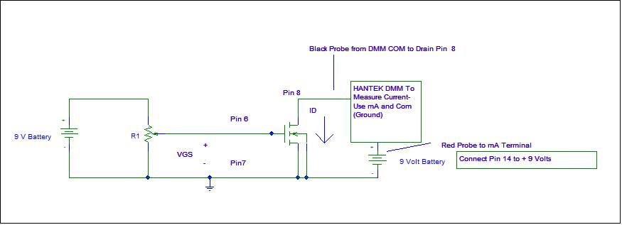
Figure
6.2 Circuit Used To Extract VT and k.
·
You will be using the HANTEK DMM to measure VGS and ID for
each data set.
·
You will be able to adjust VGS from 0 to +6 volts by using
the 10K or 100K potentiometer
·
You will have to switch the DMM Red and Black test leads from setting and measuring
VGS and measuring ID between the Voltage Input and the mA current input.
·
VDS is essentially a constant at +9 volts.
·
Verify that Pin 14 is connected to +9 volts as shown in Figure
6.2
·
Use the DMM to verify the potentiometer value you are using.
Ø Adjust and measure VGS from 0 to 6 volts in
1-volt increments and for each VGS, switch the red lead from the VGS measurement to the mA input and measure ID. You could use 0.5 volt VGS steps between VGS
= 3 and 6 volts to improve accuracy.
Because the potentiometer is hard to adjust to exact values, you should
use whatever makes sense.
Ø Record VGS and ID to an EXCEL spread
sheet. Graph SQRT(ID)
versus VGS and extract values for VT and k.
Ø Build a SPICE model using your values of VT
(VTO) and k where KP in SPICE is =2xk.
Refer to 19 and 21 October Class Notes.
A
holdover from our LED discussions

Now
to assist with your mathematics and physics:

How I feel about WINDOWS 10
on my DELL computer.