EE 2212
EXPERIMENT 6
4
November 2021
NOTEBOOK REVIEW
MOSFET I-V Characteristics
NOTEBOOK REVIEW:
We will use the first hour or so for individual reviews of your
notebook; the remaining laboratory time will be for the MOSFET I-V
characterizations.
Ø The intent is to model the notebook review
as if we were having an industrial design review; that is a review that is
constructive for every one concerned. Discussion is strongly encouraged. We are all in it together.
Ø In alphabetical order based upon my class
list for each lab, I will ask to “see” your notebook. That is you will display selective pages of one or more of the
five experiments to date. Be sure your
imaging systems in whatever platform you are using IS OPERATIONAL!
Ø I will evaluate your work on a CHECK PLUS
(Exceeds Expectations), CHECK (Meets expectations). CHECK MINUS (Does not meet
expectations) rubric. The evaluations
will be confidential.
Ø I anticipate each of the reviews will require only 2-3
minutes, consequently we should complete the review in an hour or so leaving
two hours for the MOS Lab.
Ø I am using typical Intellectual Property
guidelines acceptable in patent filings.
I expect to see a Table of
Contents, URL where your computer files are kept, dated entries for when the
work was done, circuit diagrams, comments and conclusions, essentially
following the guidelines in the LabInfo.docx LabInfo.docx document.
PURPOSE
To measure
the I-V characteristics of an N-channel MOSFET on the CD 4007
array. Enter your data:
VGS, VDS, ID in an EXCEL spread sheet and use these data for
preparing your graphs and parameterization of
the FET.
COMPONENTS
Ø CD4007 MOSFET array
PRELAB
Prepare a detailed circuit
diagrams in your notebook of how you will connect an NMOS for measuring the I-V
curves and how you will connect the inverter circuits. Study the material in Chapter 4. A complete
manufacturer’s data sheet has been posted as a pdf file on the class WEB page.
The device you will use
throughout this experiment and Experiment 7 is a CD4007B Transistor array. CD4007-tiDataSheet.pdf It contains three N-channel and three
P-channel devices connected as shown Figure 6.1. Detailed schematic diagrams and pinouts are
available on the data sheet and also given below,
Please use care when
working with these chips. They are very susceptible to excessive voltage and
ESD (Electro-Static Damage).Avoid handling by the pins. Remember to touch a black lead (ground) of
one of the BNC cables connected to the oscilloscope or signal generator or the
ground terminal on the power supply before you start wiring your circuit. This time of the year often has low relative
humidities which make ESD more of an issue. Do not exceed the experiment settings in an
attempt to make your experiment work. The pin configuration is
given in Figure 6.1. Note that you will
be using the CD4007B which have a lower maximum voltage rating than the
CD4007UB. The diagrams are the same for
both the “B” and “UB” suffix devices. Study
the I-V curves, Figure 5, provided in
the data sheets CD4007-tiDataSheet.pdf so that you have some idea of what to
expect. Also study the chip circuit
diagram. You should be able to identify
the operation and function of all of the individual devices. Observe the input protection circuitry, D1
and D2, that we
discussed in class.

Figure 6.1 Pin Configuration of CD4007.
Warning: Pin 14 should always be connected to the
most positive dc voltage in the circuit.
Pin 7 will always be connected to the most negative dc voltage in the
circuit
(or else ![MCBS00726_0000[1]](Experiment6MOSCharacteristicsAndNotebookReview_files/image016.gif) )!!!
)!!!
PROCEDURE
I-V Characteristic of an
N-channel MOSFET
Ø Connect the circuit shown in Figure 6.2. Use
the NMOS connected to pins 6 (GATE), 7 (SOURCE), and 8 (DRAIN). Remember to also connect pin 14 also to the
+VDD supply. Pin 7 is shown connected to ground, VSS = 0. Although you can use the built-in mA meter on the power supply to
measure ID , a better way yielding better accuracy is to measure
current by measuring the voltage drop
across a 1000 Ω resistor
connected from Pin 8 to Pin 14 and realizing that ID = V(across the resistor)/1000Ω.
Ø Do not use the digital multimeter to measure current because of the hassle in
replacing the internal fuse. Use the
voltage readout on the power supply as you sweep VDD from 0 to 15 volts for each value of VGS from 0 to 6
volts in 1-volt increments. Measure VDS
and ID for each value of VGS using the multimeter. Note that the threshold voltage, VT , is in the 1 to 2 volt range. Refer to the data sheets where similar curves
are illustrated. Record data in an
EXCEL spread sheet.
Ø 
Figure 6.2 ID-VDS As A Function of VGS
Characteristic Measurement For an NMOS
Ø Note that you should keep below ID
= 10mA; since
this is the maximum rated value for this chip, consequently you may not be
able to use all values of VGS depending upon your chip. Plot
VDS and ID data as you
proceed. Record data in an EXCEL
spread sheet. Using an EXCEL spread sheet and extracting graphs from the spread sheet
is a good way to display and understand the data.
Ø The CD 4007, as
are most MOS ICs, is unforgiving for ESD and over voltage and over current.
Ø Plot your data and use a linear regression
(least squares fit) to extract values for VTO, LAMBDA, k, and KP and develop a
SPICE model that compares with your measured curves. An EXCEL spread sheet works well and yields
nice graphs. The objective is to obtain
ID versus VDS for several different values of VGS. Look at Figures 5 and 8 on the CD 4007 data sheet as a guide
as to what to expect. You will have to
assume W/L=1 because you do not know the actual values of W and L and then
adjust KP accordingly. This model
development from your parameter extractions should be included in your report.
Develop a Shichman-Hodges model equation for your NMOS.
Ø Observe that SPICE syntax for Kn’ (for an NMOS) and Kp’ (for
a PMOS) is KP, independent whether you are modeling an NMOS
or PMOS. Refer to Table 4.2 from the
text.
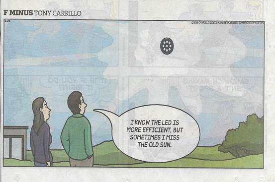
A
holdover from our LED discussions
Now
to assist with your mathematics and physics:
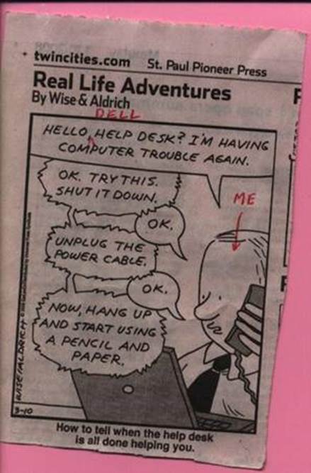
How I feel about WINDOWS 10
on my DELL computer. And now WINDOWS
11!!!