EE 2212
Spring 2019
14 February 2019
Experiment 3: Additional Operational
Amplifier Circuits
Purpose
To
simulate and implement
the designs of:
Ø An active analog Low-Pass Filter (LPF)
Ø An active analog High-Pass Filter (HPF)
Ø An active analog Band-Pass Filter (BPF)
Ø A Wien Bridge Oscillator
GENERAL COMMENT
Run SPICE
frequency domain simulations with a VAC generator programs for the LPF, HPF,
and BPF. Use the μA741 model in the eval.slb library.
You will need the following information from your SPICE program in order
to complete this lab:
Ø AC
analysis including amplitude as a function of frequency from around 10 Hz to at
least 10 kHz.
Ø TIME
DOMAIN ANALYSIS IS NOT REQUIRED!
PRELAB
Use your design for the
inverting operation amplifier with a low frequency voltage gain of 20 dB from Experiment 2, Figure 1, as a basis to implement your
design.
Figure 1 (Refer to Experiment
2)
Design the Low Pass and High Pass
Filters to meet the indicated specifications. You should come to the lab with a
list of the components you will need to meet the specifications. For the
Low-Pass Filter, Figure 2, the corner frequency is computed from 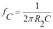 and the low frequency
voltage gain is given by
and the low frequency
voltage gain is given by 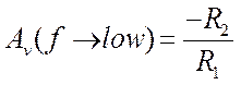 and for
the High-Pass Filter, Figure 3, 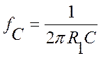 and the high frequency
voltage gain is given by
and the high frequency
voltage gain is given by  . The derivation of
the corner frequencies follows that of the passive RC filter circuits from
Experiment 1 and from class last week.
We will also discuss more at the beginning of the lab period. Include the derivations in your notebook.
. The derivation of
the corner frequencies follows that of the passive RC filter circuits from
Experiment 1 and from class last week.
We will also discuss more at the beginning of the lab period. Include the derivations in your notebook.
PROCEDURE
Refer to the mA741 data sheet. Observe, again that you
are using the 8-pin DIP. Do not include
the 10 kW offset
voltage potentiometer. All resistors must be at least 2 kW. Use ± 12 volts for the power supplies. Your
Low Pass and High Pass designs should be supported analytically and by SPICE
simulations. Use the library model for the mA741.
Adjust your input levels to avoid otput
voltage clipping.
1.
ANALOG ACTIVE LOW-PASS FILTER
Design
and test an low-pass filter with a low-frequency voltage gain of 20 dB and a 3
dB corner frequency in the range of 2
to 4 kHz,
Figure 2. Do not use series and parallel capacitor combinations or series and
parallel resistor combinations . Use standard values that yield a corner frequency and voltage
gain reasonably close to the specifications.
Ø Experimentally verify your design and
simulation results.
Ø For verifying low-pass filter operation,
measure 20 log|A(jf)| and compare your results
with the SPICE AC simulation over a similar range.
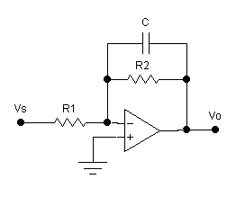
Figure 2 Low Pass Filter
2. ANALOG ACTIVE
HIGH-PASS FILTER
Design and test
a high-pass filter, Figure 3 with a high-frequency voltage gain of 14 dB and a
3 dB corner frequency in the range of 50 Hz to 200 Hz. Do not use series and parallel capacitor
combinations or series and parallel resistor combinations. Use standard values that yield a corner frequency and voltage
gain reasonably close to the specifications
Ø Experimentally verify your design and
simulation results.
Ø For verifying high-pass filter operation,
measure 20 log|A(jf)| and compare your results
with the SPICE AC simulation over a similar frequency range.
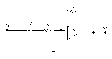
Figure 3 High Pass Filter
3. ANALOG ACTIVE BAND-PASS FILTER
Now cascade the output
of the HPF with the LPF and note the band pass characteristic. Measure
20 log|A(jf)| and compare your
results with the SPICE AC simulation over a similar range. The center of your filter design will peak
near 34 dB or about |Av| approximately50. You will have to adjust your input level to
avoid output voltage clipping.
Figure 4
Band Pass Filter
4. WIEN BRIDGE
OSCILLATOR
So far, all of the
circuits we have studied employ negative feedback. The following circuit, Figure 5, employs positive feedback; and as mentioned
in class, an audio example of positive
feedback is the “howl” observed when the microphone and speaker are not placed
well in an auditorium and you have constructive (additive) signals; positive
feedback. Construct the following
circuit which is similar to what is shown in Figure 12.43 on page 741 of the
text. At first glance, the circuits look
different but they are the same. You are
generating a signal source, that is you are
demonstrating the operation of an oscillator.
Observe that there is no external signal generator!!!! Monitor vo(t) using your oscilloscope.
Observe there is no input signal.
This is called a Wien Bridge Oscillator. Explain why this is a useful circuit. (Note depending upon the resistor tolerances
and circuit losses, you may have to increase your value of R2 somewhat; perhaps
as high as 33 kΩ). Lead dress has
an impact on the circuit performance.
Compare the observed oscillating frequency of operation to the equation,  and the voltage gain
required setting established by
and the voltage gain
required setting established by .The SPICE simulation approach is interesting and I will
demonstrate this when your group reaches that part of the lab. In a real circuit, an oscillator starts
through random noise which provides an initial signal with the correct phase
shift to obtain positive feedback . To show this in a SPICE simulation, add an
initial condition of several tenths of a volt to each of the capacitors as an
initial condition and then use a transient analysis that extends for several
periods of the expected frequency output.
The exponential signal growth is kind of cool (at least I think so) to watch during the
simulation. The simulation makes you a
believer in the exp(+αt) DFQ solution.
.The SPICE simulation approach is interesting and I will
demonstrate this when your group reaches that part of the lab. In a real circuit, an oscillator starts
through random noise which provides an initial signal with the correct phase
shift to obtain positive feedback . To show this in a SPICE simulation, add an
initial condition of several tenths of a volt to each of the capacitors as an
initial condition and then use a transient analysis that extends for several
periods of the expected frequency output.
The exponential signal growth is kind of cool (at least I think so) to watch during the
simulation. The simulation makes you a
believer in the exp(+αt) DFQ solution.
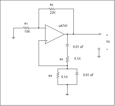
Figure
5 Wien Bridge Oscillator

Alternative definition for
mobility
And micrometer
$1500 for a 512 GByte XsMax

Do you believe this
explanation or the one claiming the WEB originated
as a
spin-off of a U.S. Department of Defense
ARPANET project?
Time to start thinking about out of EE technical
electives registration for next semester.


Also UROP, Deadline Coming Up Soon