EE 2212
EXPERIMENT 10
15 April 2021
THE EMITTER-COUPLED PAIR
PURPOSE
Note 1: Experiment 10 will
not be collected but I will look for the work in your Laboratory Notebook. A comprehensive notebook review is scheduled
for Thursday, 22 April.
The purpose of this experiment
is to characterize the
properties of an emitter-coupled pair:
·
DC
Biasing
·
Time
Domain Measurements
COMPONENTS
Ø
LM3046/CA3046
transistor array. The data sheet is also
posted on the class WEB page LM3046NationalSemiconductor.pdf This is the IC you
used last week.
Ø
47
kW resistor for each collector
Ø
REE
for you to design for DC biasing. We do not have an infinite variety of
resistors which means you will have make reasonable adjustments to the design
specifications.
GENERAL INFORMATION
Ø Figure 10.1 is a pin out of the
LM3046/CA3046/3045 Transistor Array. Observe that you MUST connect Pin 13, the
IC substrate, to
the most negative point in the circuit or bad things happen to the IC. The most negative point is the VEE-REE
node, not ground!
Refer to Figure 10.2

Figure 10.1 LM3046/CA3046/3045
NPN BJT ARRAY
Use Figure 10.2 and class notes for guidance to
prepare a detailed circuit diagram. Include pinouts
for the LM3046/CA3046 npn array. From your circuit diagram and circuit
specifications, calculate the expected important Q-point values and Adm
.
DC MEASUREMENTS
Refer to the diagram and data
sheet of the LM 3046/CA3046 BJT array.
Set up the circuit in Figure10.2 using Q1
and Q2 on the LM3046 IC for the emitter-coupled pair. Lead dress and length is also important. Be neat!
Design a value for REE such
that the ICQ1 and ICQ2 are about 100 μA.
·
Ground
both the inputs of Q1 and Q2. That is do not connect the HANTEK AWG for the DC
set-up.
·
Verify
that both battery packs are turned on.
·
Measure
the all Q-point voltages and currents using the DMM. Also measure the VCC and VEE voltages to be
sure there is still some battery life! Some of you had dead batteries last week. Compare
your Q-point values with the expected and SPICE simulations.
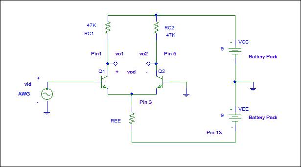
Figure 10.2
·
Compute
the expected Adm = vod/vid
for the circuit so that you can set the HANTEK AWG to a reasonable amplitude to
minimize clipping.
·
Connect
the AWG as shown in Figure 10.2. Set
f=100 Hz and the desired amplitude.
·
Connect
Channel 1 to vo1 and Channel 2 to vo2 and Auto scale.
·
Also observe that because the oscilloscope does not have a floating input (i.e., one side of each of the two oscilloscope inputs
are connected to ground), you will have
to measure either VO1 or VO2
and scale the final results accordingly by a factor of 2 and also do not
forget the sign (180°phase) difference between each of the outputs.
·
You can not connect one probe across vod
because one side of the probe is grounded through the coaxial cable.
·
Observe
what happens when you increase the AWG signal input level.
·
Compare
your results to a SPICE transient simulation and analysis.
A bit of EE humor.

This guy deserves a tip!

And for those of you who go to
Buffalo Wild Wings and
try their “Blazin”
ghost pepper suace

You might cover conformal
mapping from an advanced math course
when using Smith
Impedance Charts
in EE 3445 or the Antenna and Transmission
Line Course
