ECE4311 Cadence Tutorial
1. Introduction
The objective is to give a tutorial to circuit designers who would like to get acquainted with Cadence design tools (version 5.1.4.1) for VLSI custom design. A step by step tutorial approach is adopted. It is the hope that by the end of this tutorial session, the user would have known how to create a schematic, perform simple manual layouts and, of course, run simulations.
Those of you who have some basic knowledge of Cadence tools already may prefer to jump ahead to your desired topic without fearing the loss of continuity. There is also a possibility that you have a different technique to implement the same steps described in this tutorial, which may be more efficient. However, this tutorial is a good way of getting started with Cadence for a person who has never used it before or long time before.
Cadence, like most other complicated and powerful software tools, runs best on UNIX/LINUX operating system. In case you are not familiar with UNIX/LINUX, check out basic commands at the following website (or refer to that website when needed):
http://www.ill.fr/lss/unix/unix_tail.html
2. Setting Up Your Unix Environment
Cadence can be run only on UNIX terminals or PCs loaded with UNIX terminal
emulators like Exceed. You need to have a VLSI account for this version of Cadence. Cadence is only installed on
the UNIX machines located in the ECE Department room MWAH 295. This room is
also known as the VLSI Design Laboratory.
Off-campus logon to these terminals is not
possible for security reasons.
There are 12 computers now in VLSI lab. Some are running Sun Solaris 9/10 operating systems and others running Windows. If you find that you are using one of those WINDOWS machine, you would need to use Exceed to emulate a UNIX terminal. To do that, click program, then find Open Text Exceed 14×64, then click on it, go to Exceed Tools, and finally click Exceed XDMCP Query.
The first time when you login, your username is login name of your UMD email and password is ‘welcome’. Once you login, I suggest you change your password. First, close all those windows after you login. Then right click, go to Host and then Terminal Console. Once a Console window pops up, type passwd and follow it to change the password.
Before you can start Cadence, you need to include some information to locate the cadence libraries and setup files. This will be done by including a statement in your .cshrc file as mentioned in step 1 below. You can also have your own personalized settings in your home directory for the setup files, if you like and you are familiar with UNIX/LINUX operating systems.
Setting up the Cadence Environment
1. Suppose that the .cshrc file is properly configured, now if you desire to invoke cadence, you will need to make sure that the above change in .cshrc file takes effect. This is automatically done, everytime you logon to VLSI account. However, if you desire that the new changes take effect immediately in the same session, you will need to execute source .cshrc at the command prompt.
2. Copy the following graphical interface related files to your home directory. (Note: your home directory is the directory where you initially logon, it should look like this /home/usra/ece4311/fall011/username). You can type ‘pwd’ to show the current directory you are in at any time. Note that in UNIX/LINUX systems, the symbol ‘~’ can be used to stand for the home directory. We will be using this a lot below for simplicity.
A) From a terminal prompt, create a new directory from your home directory called cadence/ece4311 by typing the commands shown below. This is where you’ll organize all your Cadence files and directories for ece4311 class.
mkdir cadence (there is a space after the command)
cd cadence
mkdir ece4311
mkdir models
B) Copy some important setup files to your home directory.
cd ~ (~ stands for
home directory)
cp /home/research/thua/ece4311_files/.cshrc ~/
cp /home/research/thua/ece4311_files/.cdsinit ~/
cp /home/research/thua/ece4311_files/.cdsenv ~/
C) Copy the file cds.lib to your working directory.
cp /home/research/thua/ece4311_files/cds.lib ~/cadence
Note: the above commands are UNIX operating system commands.
3. Copy the model file. For this tutorial, we will be using TSMC 0.25um technology. There are two model files in this case, one named tsmc25N.m for NMOS transistors and the other tsmc25P.m for PMOS transistors. They are located at /home/research/thua/ece4311_files as well. Type the following command from a terminal prompt to copy those two files to your local path:
cp /home/research/thua/ece4311_files/tsmc25*.m ~/cadence/models
then, you should see a directory named models under ~/cadence.
your model files will be there in the sub-directory models.
There
is one more thing to do before we start Cadence. There is a file called display.drf.
This file is very important: it defines
all the color templates or patterns for different layers in the layout. You
need to copy that file to the directory where you will start Cadence, in this
case, ~/cadence.
So, do the following:
cp /home/research/thua/ece4311_files/display.drf ~/cadence
Now, you are ready to start running Cadence
Software. But note that it is suggested that you start Cadence under ~/cadence directory. In this way, you maintain a
good structural organization of all your files.
3. Starting Cadence
Note: close the terminal where
you worked on part 1 and 2. Start a new terminal before you work on part 3. In
that way, the .cshrc file is sourced automatically and will be in effect.
After you have the complete setup for the cadence ready in your VLSI account as described in the previous section, you are now set to begin your journey with Cadence.
Follow the following steps to setup your own cadence directory, and to start cadence.
1. In your home directory (~/), change to the directory in which you want subsequent Cadence files to be stored in. To do this, execute the command at the UNIX prompt: cd ~/cadence
2. To start Cadence, type the following at the UNIX prompt:
icfb &
Sometimes, it takes a while before the Command Interpreter Window (CIW) appears and is especially so when the workstation is bogged down. An example of how the CIW looks like is shown in Figure 1 below:
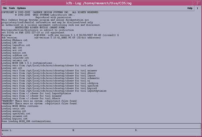
Figure 1. CIW window
When all the configuration files have been read, the following message Done Loading NCSU_CDK Customizations will be displayed indicating the start up was successful. With each new session, Cadence starts a new CDS.log file in your home directory where all the messages that appear in the CIW will be stored. Along with the above window, you may also see the Library Manager Window, which lists all the libraries for your design. If you do not see the window, click on Tools in the CIW window, and then select library manager.
The Library Manager Window will look like as shown below in Figure 2. Note that the NCSU_TechLib_tsmc03 technology library should appear under the column library. Make sure that there is no any warning in the bottom message pane. If there is, something is wrong with your cds.lib file. (Note that the content in your library part may not be exactly the same as those in the figure, since I am using my Cadence account for an illustration!)
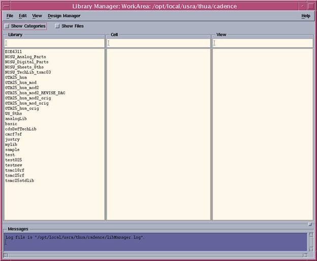
Figure
2. Library Manager Window
If, at anytime during this tutorial, you want to quit Cadence, make sure you save your work by selecting Save from the Design menu and close the design windows by selecting Close from the Window menu. This will become clear in the sections to follow. After you have closed all your work windows, click on Exit from the File menu in the CIW window. A following window will pop up.
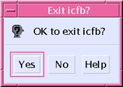
Click on the Yes button and you're done with the Cadence session.
From now on, a simplified convention will be used to show the sequence of options used from the pull down menu. For example, File --> Exit will indicate that you first open the pull down menu for File and then click on Exit. Another example could be Tools--> Analog Artist --> Simulation, which will indicate that you need to pull down the Tools menu first, then click on the Analog Artist button and finally click on the Simulation button.
4. Create Libraries
When starting a design in Cadence, the first thing to do is to create a library where you can store your designs. Every Library is associated with a technology file and it is the technology file that supplies all the color maps, layer maps, design rules, extraction parameters required to view, design, simulate and fabricate your design.
Let's go through the steps of creating a library, one by one.
1. From the CIW window, open the library manager. (Again, if you didn't have the library manager window at the first place, you can open it by going to the CIW window and clicking on Tools-->Library Manager). Then, click on File-->New-->Library. You will see a window popup as follows.
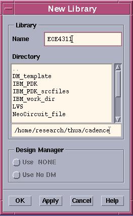
Enter the name of library (example shown: ECE4311) where you expect to store your own designed cells. Note that the Directory entry shows ~/cadence, where you started Cadence and this will be where your library is stored. Remember that you had already created ~/cadence as a directory in the section on Starting Cadence. Finally, you should click on the OK button in the above window. A window pops up that will ask you whether you want to attach or compile a technology library to it. Choose to attach a technology library and click OK. Then in a new pop-up window as follows, select NCSU_TechLib_tsmc03 as the technology library (it may already is) and click OK.
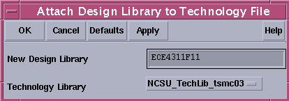
This would mean the created
library ece4311 will contain circuits made of
technology NCSU_TechLib_tsmc03.
Finally, note a few messages in the CIW window. One of the messages
should be Library Creation Successfully Completed. This will ensure that you have created a library ece4311 in the ~/cadence/ece4311
directory.
2. Now, if you look at your Library Manager Window, you should see ece4311 as one of the libraries in the left most column. Click on ece4311 and you should see no cells, because you have not made any circuit cells yet.
5. Create Schematics
At this point, you have created a library of your own and can begin the design process. For a full custom design, the process begins by creating a schematic, simulating it (whether in Verilog, Spectre or HSpice) in order to optimize the performance, and then comes the layout (which is where you flaunt your artistic skills!). After the layout is completed, you need to extract the layout and compare it with the original schematic - a process called Layout Versus Schematic, in short LVS verification. You will then perform a final simulation on the extracted layout, which includes parasitic capacitances. The post layout simulation result is closer to reality and gives you a good idea of whether your design would work if fabricated. In this section we would be talking about creating your own Schematics.
1. To create a schematic, click on File-->New-->Cellview in the CIW window. You could also click on the File-->New-->Cellview in the Library Manager Window to create a schematic. A pop-up menu will appear as follows.
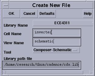
Click on the library name button and select ECE4311. Then click on the Tool button to select Composer-Schematic (by default it is). The View name will automatically change to schematic. Enter the name of the cell you wish to design in Cell Name field. For the tutorial case, let’s design an inverter. This will pop-up an empty Schematic Creation Window.
2. You need to bring devices into your design in this window. The following schematic shows how to connect NMOS and PMOS devices to make an inverter, which is what you are aiming for in this tutorial.
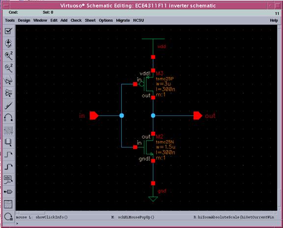
Figure 3. Inverter Schematic
The
following steps will teach you how to create a schematic like the one shown
above:
3. To place an instance, e.g. an NMOS device, on your schematic, first move your mouse so that the arrow is in the schematic window, then type i (must be lower case) and wait for a while. Alternatively, you can click Add-->instance. A Component Browser window will appear along with another pop-up menu. Go to the Component browser, which looks like this in Figure 4 below.
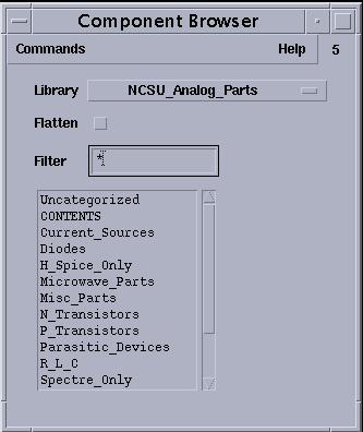
Figure 4. Component browser Window
The above window is asking you which instance to add into the schematic window. Click on Library first. Note that this will pop up a library pane to let you select the library. In our example, Click on NCSU_Analog_Parts in the Library pane. Then Click on N_Transistors in the Filter field, and this would help you narrow down to the instance you want. After you click on N_Transistors, note that the field changes to NMOS transistor instances only. In our example, we can just select the instance by clicking on “nmos”.
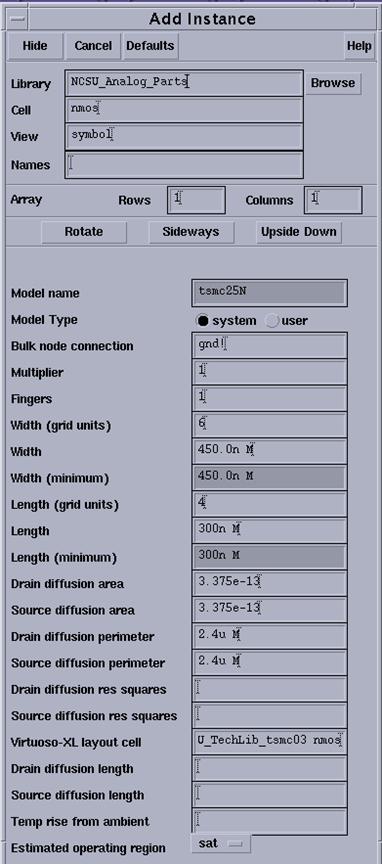
Notice that now your selected instance will pop up an Add Instance window along with its initial default parameters (such as the width, length etc) as shown above. Now, move the mouse to the Schematic Editor window and you will see a yellow instance of the nmos to be placed. To place the instance, click on the left mouse button. Another new instance will immediately become ready to be placed. If you need an additional NMOS transistor, you can re-click the left button in the Schematic Editor window. Press ESC to stop adding anymore NMOS devices. Note that then the Component Browser window will disappear along with Add Instance window. (Note: ESC is the key to escape from Cadence's persuasive nature. If you don't want Cadence to do what it is doing right now, you can always press the ESC key. Most of the times, cadence will yield to your requests).
To set the properties of the instance that you just placed, e.g. the width and length of the NMOS device, move your cursor on top of the device and type q. An Edit Object Properties window will pop up. Fill in the value for the Length property by deleting whatever there is in that entry, and then entering the proper length using the scientific notation of u as shorthand for microns, in this case it would be 0.3u. As soon as you enter the properties, an M will appear automatically and it will look like 0.3u M. Follow the same procedure for the Width property and change it to 0.9u. You can also enter other properties in an analogous fashion, if desired; otherwise the default values will be used.
4. Repeat
the above step 3 to add a PMOS transistor instance (in this case select pmos
from the NCSU_Analog_Parts library) and make its width 2.7u. Note: the body of the NMOS should connect to
negative-most voltage (GND in this case) and that of PMOS to positive-most
voltage (VDD in this case) in order to back-bias the PN junction at source and
drain region, as discussed in class. So, now if you look into the properties of
both transistors, you notice that by default the bulk node connection is
already set to either gnd! or vdd!)
5. To place
a wire to connect the two devices as depicted in the inverter schematic above
(the blue lines), move your cursor to the point where you want the wire to
begin. Then type w and move
your cursor. You will see a yellow line
connecting the starting point and the cursor. Click the left mouse button
at the point where you want to change the direction of the wire. Wire the
PMOS and NMOS devices as shown in the inverter schematic above. After this,
select vdd and gnd from the library named analogLib to connect the global power
sources.
6. The next step is to specify the input and output pins (the red colored polygon). With your cursor in the schematic window, type p and a pop up menu will appear.
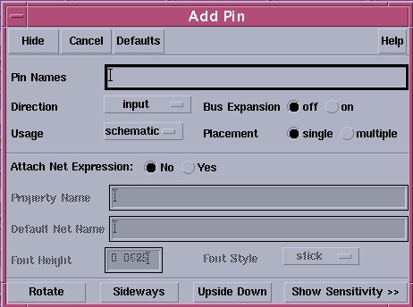
We will specify the input pin first. In the Pin Names field, type in. The Direction is input and the Usage is schematic. Then move your cursor into the Schematic window and you'll see the pin in yellow outline. Click on the left mouse button to place the pin. We'll now specify the output pin. Move your cursor back into the pop up menu and type out in the Pin Names field. This time, however, the Direction is output. Again place the pin at the desired location.
7. You have just completed your first schematic in Cadence. To check and save your design, click on the first icon to the left of the schematic (it is the icon with a box and a check mark). You need to check for any error/warning messages in the CIW window if you have any error/warning (such as floating wires or pins). You can also perform the same function by selecting Check and Save from the Design menu of the Schematic window. To close the Schematic window, select Close from the Window menu in the Schematic window or simply double-clicking the upper left.
QUICK
USAGE REFERENCE: (any short key below and
much more has a corresponding menu in the window)
1. Press
'p' to add pins
2. Press 'q' on the device/instance to edit properties for the device
3. Press 'w'
to add wires
4. Press 'f' to fit the schematic in your schematic window.
5. Press 'l' to label a wire.
6. Press 'Up' and 'Down' arrows to move up and down within a schematic window.
7. Press 'ESC' to terminate any of the operations in the schematic window.
6. Create Symbols
Symbols are useful when creating designs where it is impractical to show every transistor on the top level schematic (i.e. hierarchical designs). Instead, symbols of the cells are created in order to instantiate them in the higher-level schematics and make them more readable. In this tutorial, we will create a symbol of the inverter.
1. From the Design menu in the Schematic window, select Create Cellview -->, From Cellview...
A pop up menu will appear. The default information shown in the menu will most likely to be what you want. An example of the menu is shown below.
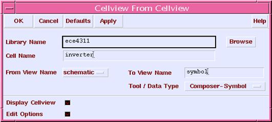
Click OK will pop-up another window, which will contain a default symbol
picture. Usually it is a rectangle with red square dots for in and out
pins. This symbol view is created under the cell you are editing. A more
meaningful symbol can then be generated by editing the symbol view itself, but
this would be lost if the symbol generation program is run again. An
example of an inverter symbol is shown below.
![]()
![]()
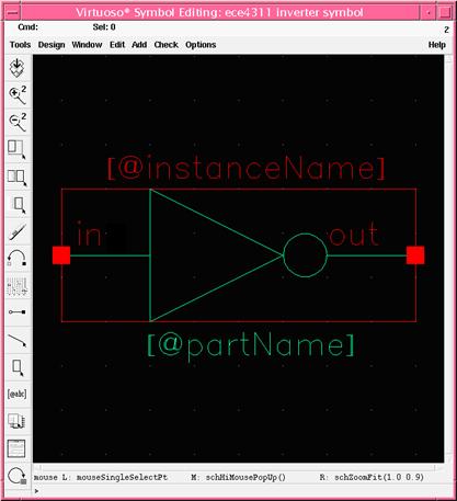
How do we get a picture like that? First, let us review what the figure look like. It has a red box which encloses the green colored inverter symbol. This red box defines the actual size in terms of a rectangular box that a symbol will occupy, if you were to use this inverter in another design. You can change the size of this box. It is good custom to exactly fit the symbol within the red box. The red square dots indicate the pin connections. [@InstanceName] and [@PartName] are display variables, which you may delete or keep.
2. If you
want to move any object, just move the cursor on top of the object and type
m. The object will then move with the
cursor. Or you can select the objects to be moved by drawing a box around
the objects. This can be done by clicking and holding on to the
left mouse button while you draw the box. After highlighting the objects
to be drawn, type m and the highlighted
objects will move with your cursor. Likewise, if you want to delete an
object, move the cursor on top of the object and hit the
3. To draw a
line, move your cursor to the Line icon (the
icon with a descending line) and click on the left mouse button. Icons
are to the left of the symbol window. Move your cursor to the location
where you want to draw a line and click on the left mouse button. If you
draw a closed object, all you have to do is to click on the points where you
want to change the direction of the line. However, if you're drawing just
a straight line, you need to double click the left mouse button on the end
point of the line to signify the completion of drawing the line.
4. To draw a circle (or any other shape), first click on the Line icon and then click on the Cmd options icon (the second last icon). A pop up menu will appear. Select the Shape as circle by clicking on the diamond button as shown below.

Then move your cursor to the location where you want to
draw the circle and click on the left mouse button. That is the center of
you circle. Move your mouse so that the circle is as big as you desire it
to be and then click on the left mouse button again. To move the circle
to the desired place, follow the procedure mentioned in step 2 above.
5. You
have completed your symbol. To save your work, select Check and Save from the Design
menu in the symbol window. You may also save your symbol design by
clicking on the Save icon which is the first
icon.
6. To close the symbol window, select Close from the Window menu in the symbol window.
7. Simulation with Spectre
In this section, we will perform transistor level simulation for an inverter schematic we designed earlier in the tutorial using spectre simulator from Cadence.
1. Before we can simulate the inverter, we will need to specify power supply voltages and input stimulus to the inverter. There are two ways of doing this. One method is to create a stimulus file and the other is by creating another schematic called the test schematic. We will concentrate on the second method in this section. This method enables you to test module by module for a big design.
For an inverter, create another cell called 'inverter_test' in your current library 'ece4311'. We will always consider our current library to be 'ece4311'. This is in addition to the inverter, which you had already created earlier. Create a schematic view within this cell. Refer to " Create Schematics " section of the tutorial on how to create a schematic. For your convenience, the steps are mentioned again. You would be clicking on File --> New --> CellView in either the CIW window or Library Browser window. Then you would enter Library Name as ece4311, cellname as inverter_test and View Name as Schematic. This should pop-up an empty Schematic Editing window. In this window, you will generate a final schematic as follows.
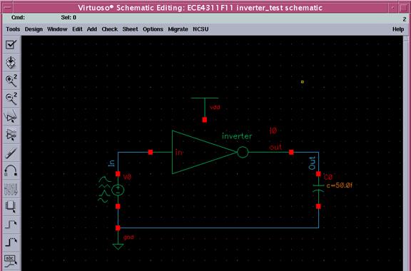
To generate a schematic like this, you will need to go through the following steps. This assumes that you have already had an inverter schematic and its symbol.
1 a. Place an instance for an inverter. (how to place an instance has already been discussed in " Create Schematics" section). Make sure that you choose an inverter symbol from the ece4311 library as your instance.
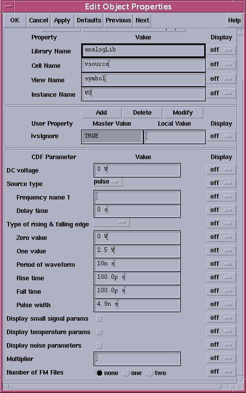
1 b. Place an instance for the vsource, which you can find in the analogLib library. Enter it's properties, such as a periodic pulse-like waveform so that this is going to be your input to the inverter. You can select pulse in its properties window and set the properties as you do in SPICE. Give a finite rise time and fall time. For example, as shown in the following Edit Object Properties window, I was specifying a pulse with 10n period and 0.1ns of rise and fall time, and 4.9ns of on-time duration. Zero value means the value for logic 0 and One value means that for logic 1.
1 c. Place an instance of a capacitor, which you can find under analogLib. A capacitor will simulate the effect of capacitive loading from the following gates. Choose a value of say 100f for the capacitor.
1 d. Place a gnd symbol for ground.
1 e. Place a global vdd symbol for vdd power supply.
1f. Type letter ‘l’ and an Add Wire Window appears. Type in ‘In Out’ and then move the cursor to the Schematic window to click on the input and output wires. This will give the names to those wires. If you do not do this, the system will automatically assign random names to all wires in the circuit. However, giving names would be more meaningful, especially later when you want to look at the waveforms at certain wires (or nodes).
If you notice, we have created a test circuit for the inverter, by giving it an input and having a capacitive load. If your Schematic window is already open, click on Tools -->Analog Environment in the schematic window to start simulation. Note that this tool can also be used if you were to simulate an analog circuit like an amplifier or a filter as we did in ECE3235 Electronics II class. You should see the following window. This window is the Virtuoso Analog Design Environment window.
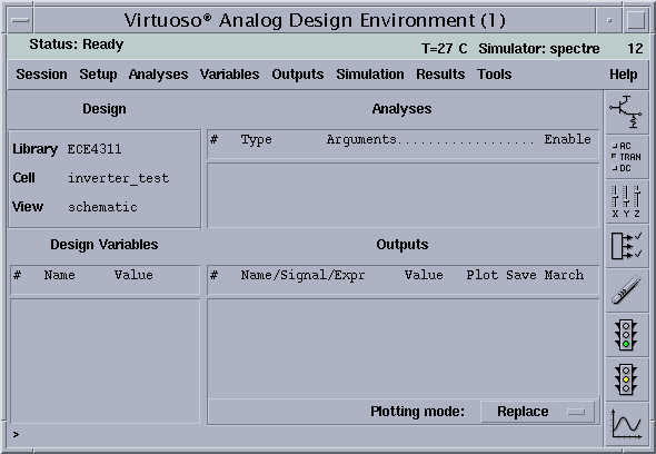
2. Verify
that that in the Design Panel you have chosen the correct design: library is ece4311, cell name is inverter_test
and View is schematic.
3. Click on Setup --> Simulator/Directory/Host . Enter the fields as shown below. Choose spectre as your simulator. A default simulation directory has also been set. You may choose any valid pathname and filename, as you like. Click ok.
4. Clcik on SetupàStimuli, and in the pop-up window select Global Sources. In the global sources window, you shall see the global voltage supply which is vdd we put in the schematic. Set its DC voltage to 2.5V power supply and check on the Enabled field. Click ok.
5. Click on SetupàModel Path. And in the pop-up window, use the Browser to select the model file tsmc25N.m and tsmc25P.m from ~/cadence//models. Click Then click on the button Add to make the model file active. Click ok.
6. From Virtuoso Analog Design Environment window, click on Analysesàchoose. A menu will pop-up. Select the type of analysis as Tran (for transient) and enter the time limits for simulation as shown below. Click Ok.
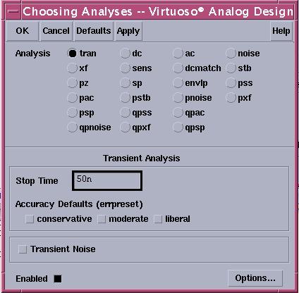
This asks the circuit to perform transient simulation
from 0 to 50 nano-seconds. Note: This is just an example. The stop time
you should give is up to how many cycles of inverter operation you want to see
and how you set your input signal vsource. Recall that I set a pulse waveform
for input with 10ns period, therefore I would be able
to see 5 complete cycles.
Click ok in the above window and then you shall see the chosen analysis is shown in the Analyses pane in the Virtuoso Analog Design Environment window.
7. Go to simulation menu in the Virtuoso Analog Design Environment window and click on Run. This will start simulation. Note that clicking Run may pop up a window showing you how to use Spectre, and just close that window.
8. The
CIW window should show "Reading Simulation
Data ...... Successful", to ensure that simulation was a success.
If not go to Simulation --> Output Log in
your Virtuoso Analog Design Environment to
find out what the problem was. Now you
can still continue with Cadence to view your result, which is mentioned below.
Go to Tools --> Results browser in the Virtuoso Analog Design Environment Window. A highly
resourceful graphical user interface to view simulation results appears as
follows.
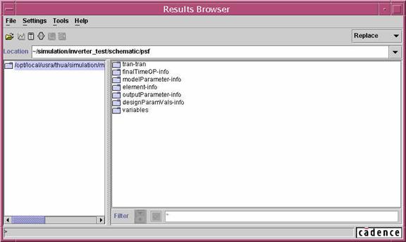
9. Select first the analysis, tran-tran in this case, and then it will show all the nodes in the circuits. Click on the input node first, then press right button of the mouse. Select calculator from the pop-up menu. A new window appear similar to the following window:

just click eval to show the waveforms. You can repeat this for all other nodes for which you want to view the output waveform.
Note:
(1) Since net names in this format of numerals may be
hard to trace in a bigger circuit, it is a good custom to label all the
important nets with sensible names for ease of reference. This is why we add
names to wires in the schematic window before. (2) Another way to show output
waveforms is to choose nodes before you run simulation. To do this, you can
click on output menu in the simulation window, choose then select output from
schematic, and finally click on the nodes you want to see. Those nodes selected
will appear in the section output.
10. clicked on Axes --> To strip to plot the overlapped waveforms as two different plots in the same window.
11. Finally, note that you can click on Sessionàsave state to save your current setting of simulators, models, analysis, simulation times, and even outputs. So that next time if you want to simulate your circuit again, you do not have to repeat the above process again. Instead, just load the saved state, which would be very convenient. I strongly suggest that you do this. Then, you can close the window.
8. Create Custom Layouts
By now, you would have known how to enter and simulate your designs using schematic capture and Spectre. The next step in the process of making an integrated circuit chip is to perform a layout. What is a layout? A layout is basically a drawing of the masks from which your design will be fabricated. Therefore, layout is just as critical as specifying the parameters of your devices because it determines whether yours is a working design or a flop!
There are 2 ways to doing a layout: manual and automated. Manual layout usually enables the designer to pack his devices in a smaller area compared to the automated process but it is more tedious. The automated process, on the other hand, is done using standard cells and usually takes more real estate space but it is much faster. In this tutorial, you will learn how to perform manual layouts of a simple inverter (we will use standard cell layouts for final project).
Before we get into the layout, first you need to understand the design rules for layout. The design rules, which we will be using, are the MOSIS Scalable CMOS Rules. It can be obtained from the following link:
http://www.mosis.org/Technical/Designrules/scmos/scmos-main.html
or use the shorter and simplified version that is given in the class or posted under course webpage.
Before we proceed any further, please make sure that your present library is associated with a techfile. Click on the library name (ece4311 in this case) in the library manager window, and right-click, choose properties. At the bottom of the window, there is a field called techfile, make sure it is NCSU_TechLib_tsmc03 (and it should be since you attached the library NCSU_TechLib_tsmc03 to the library when you created it). Note that the layout is very much process-dependent , since every process has a certain fixed number of available masks for layout and fabrication. The TSMC0.25μm CMOS process is a nwell process and supports one poly layer and five metal layers (in short, 1P5M).
1. Create a layout cellview of the cell. Here we will create a layout
for the inverter cell.
In the library manager windown, click on the File --> New --> CellView.
Choose CellName as inverter and View Name as layout. Then click on the OK button. An empty Layout editor window will
pop-up along with an LSW( called "Layer Selection
Window") window. The LSW window will show all the layers like nwell,
pwell, active etc. for the given process. An alternate way to open
the layout editor window, click on "Layout" in the View window for inverter cell
in the Library manager window. Then click on File
--> Open. A What’s New window may appear now
and you can just close it.
If the LSW window is blank, then there is an error. The LSW window should look something like this:

If LSW is blank, then the most probable error is that your library is not attached to the Technology Library NCSU_TechLib_tsmc03. You should attach you library to this technology file as described earlier on this page.
Some very important key points that might cause you trouble are listed below:
- To start the layout the first thing that you need to do is fix you grid sizing. Go to Options -> Display, the options window shown below will pop up.
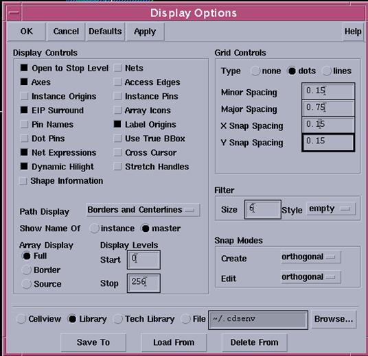
Set the grid control parameters in the right hand upper corner to the following values.

Remember λ is half the feature size so if you are using a 0.25µm (rounded to 0.3 µm) then the λ value is 0.15µm. Also, set Stop to 256 for Display Levels. Select Library on the bottom and click Save To. Once you save the options to the library, you do not have to set up the display options again when working in the same library. Click OK and then go the Window -> redraw to update new setting on the screen.
- Choose "options --> layout Editor..." from the layout editor window and make sure that "gravity on" box is checked OFF. This option ensures that you can snap your cursor to the mininum grid points and is very helpful in drawing.
- If you are facing trouble with any command, hit F3 and an option form will appear specifically for that command. You can generally solve most of the problems by choosing various options from this form which can be applied to the currently active command.
2. We are ready to draw objects in the layout window. Choose Create
--> Instance Choose
"library" as NCSU_TechLib_tsmc03,"cell" as pmos, "view"
as layout, "width"
as 2.7u (2.7u is just an example, you
should make sure that it is consistent to the width you set in the inverter
schematic). Everything else should be set by default. Take a look
at other parameters. You will see that "number of fingers" is 1 and
"length" is 300.0n (or
0.3u) which is by default the minimum possible channel length for TSMC0.25μm
technology. Shift-f and Ctrl-f will let you display and not display the layout
contents of the parameterized PMOS transistor that you have just instantiated.
Hitting Esc will cancel the command and will stop the placing of repeated
instances. Now, similarly place an NMOS with width 0.9u (again it should be
consistent to the length you set in the inverter schematic). Place it suitably
below the PMOS. At this stage, Your layout should look like as shown below :
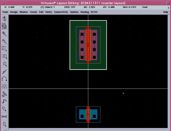
Note:
the above described way to make layout is a “lazy” way, since the layout for
the transistor is already made for you. The following description gives a more
customized way of creating layout, which involves several steps. (It would be helpful to understand the following steps by
referring to the manufacturing process discussed in class).
A
layer-by-layer approach for transistor layout (refer the above figure will help
you identify the layers to be described below and also refer to the slides
discussed in class):
(a)
since this is a n-well process, the substrate is p-sub
and this layer does not need to be put in the window since it uniformly exists
across the chip.
(b)
creating a pmos transistor layout requires a n-well.
So select n-well from the LSW window first and then choose rectangle to put a
layer of n-well in the layout window.
(c)
choose pselect layer from LSW window so that it
defines the area of the transistor.
(d)
choose active layer from LSW window so that it defines
the source/drain of the pmos transistor.
(e)
choose poly layer from LSW window so that it defines
the gate of pmos transistor.
(f)
put as many contacts (cc from LSW window) as possible
on the drain/source of the pmos. Now you should have pmos transistor that looks
like the one shown in the above figure.
(g)
Repeat the above process to create a nmos transistor
layout.
This more customized way of creating transistor layout is of
course more tedious, but tends to give better performances and more flexibility
(this will become clearer when it comes to NAND/NOR gates). I suggest that you
also try this way out to create layouts at least once.
3. Now that you have placed both
transistors, you need to make connections between them to create an inverter.
Before drawing any wires, you need to select the correct drawing layer from the
layer selection window (LSW) . First choose
"metal1" from LSW. By using create
--> rectangle or create
--> path. Note that drawing paths is a little tricky. You will
need to practice a little bit. Add in the wire connecting the drains of both
nmos and pmos which will serve as the output of the inverter. Do the same for
the poly connection between the gates (you may want to align the two
transistors vertically). This time choose "ploy1" from LSW. By using create --> rectangle or create --> path, you can also make
VDD and GND buses (VDD on top of pmos and gnd on bottom of nmos). Also connect
the source of pmos to this VDD bus and that of nmos to GND bus.
4.We also need to place substrate
and n-well contacts (recall from class why?). To place the substrate and n-well
contacts, choose create --> contact.
From the menu, you can choose any type of contact. For substrate connection you
need "M1_P" contact, and for n-well connection you need "M1_N"
contact. You also need "m1_poly" contact for connecting metal1 to the
poly gate of your inverter so that a signal on its input can come from outside
world on metal1 and directly be applied to the gate of inverter. I have
extended n-well by drawing a rectangle of nwell abutting the existing n-well in
order to cover the M1_N (n-well contact).
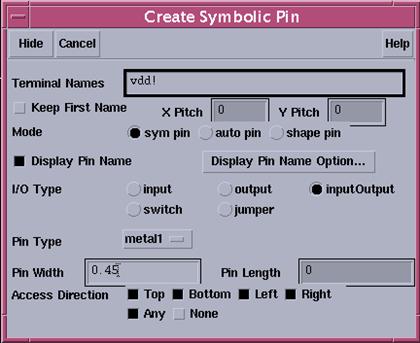
5. Select createàpin to add in pin names for the layout. The following window appers. Type in the
names in the Terminal Names field and Check on the Display Pin Name option.
Also make sure you properly set the Pin Type field (for example, if you want to
give a pin name for metal1, then you select metal1). Then move your cursor to
the layout window and you should be able click on the proper layer to set the
pin names. Note: you need to make vdd! And gnd! for the
vdd and gnd terminal in order to have LVS correct.
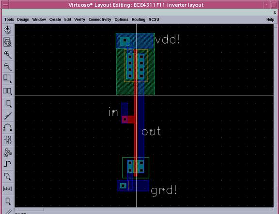
After all this exercise, your layout should look like as below (compare this layout to the inverter schematic created before to identify the connections):
9. Design Rule Check (DRC)
Our next step in the Design Process is to perform a Design Rule Check, more commonly known as DRC, on the layout. Although designers might be conscious of the design rules when performing the layout, there is a possibility of overlooking and thus violating the design rules. So, the DRC is a step taken to prompt us of any violations. This step is important because the violation of any design rules would result in a higher probability, and in some cases an absolute certainty, that the fabricated chip does not work as desired.
1. To run the DRC, choose DRC... from the Verify menu in the layout window.
A pop up menu will appear. Just click on ok.
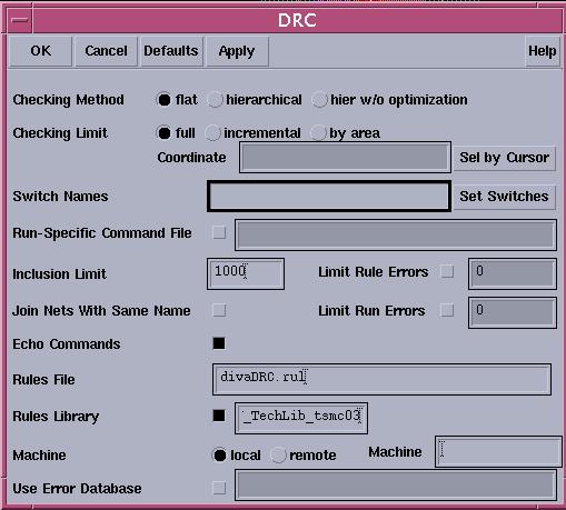
You need to make sure that you're
in edit mode for your layout that you want to run DRC on. Click on the OK button.
- Cadence then runs the DRC and reports the errors, if any, in the CIW.
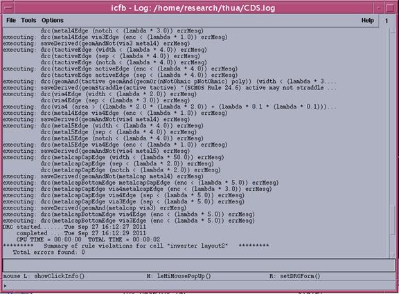
The CIW above shows that there are no errors found in the DRC process.
Note: if DRC detects an error on a layout, errors
are indicated by the markers (typically white doted areas) in your layout and it
will blink. The errors are also reported in the CIW if there is.
2 You may then proceed to correcting the errors according to the design rules if there are errors. Refer to the error report in the CIW window to get an idea what went wrong and then go to the next step to get an closer look. Then, you should probably know what really went wrong.
3 When performing huge layouts, the blinking marker might not be easily located at times. Fortunately, Cadence has an easy search tool. Under the Verify menu in the layout window, choose Markers --> Find...
A pop up menu will appear. Check on the Zoom to Markers box.
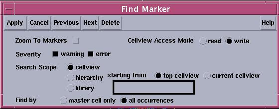
Click on the Apply button and Cadence will zoom in to the errors or warnings as desired.
10. Layout Versus Schematic (LVS) Verification
A successful DRC ensures that the layout passes through the rules designed for faultless fabrication. However, it does not guarantee if it really represents the circuit you desire to fabricate. In our case for an inverter, we really need a tool which can compare our layout with the schematic and ensure that it is really a layout for an inverter. One way Cadence does this is by generating a spice netlist from the layout and comparing it with the spice netlist for the schematic. This is the essence of the the LVS tool.
1. From the layout window, choose Extract... under the Verify menu. A window will pop-up. Make sure that the entries are as given below. For the entry in Switch Names, Click on Set Switches. A window will pop-up. Choose the option for Extract_parasitic_caps. Finally click on OK.
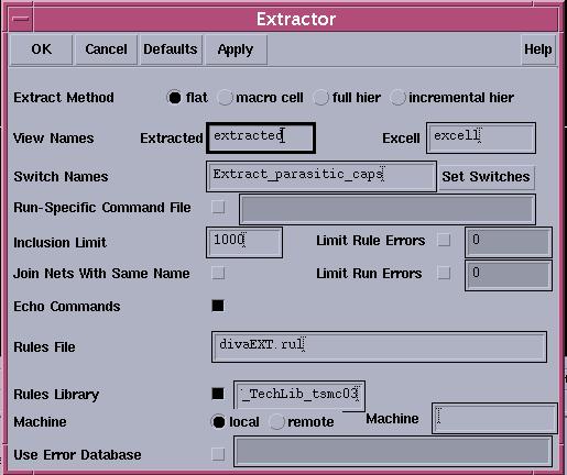
Make sure that your layout window is in Edit mode.
- Your layout will then be extracted and while Cadence is doing so, the intermediary steps will be displayed in the CIW. It will tell you whether the extraction is successful or not in the CIW as follows:
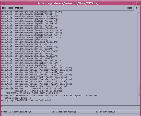
3. a. Open the extracted view of the cell in edit mode. The extracted view will look something like this.
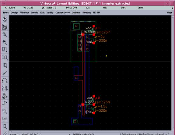
Just for fun, if you zoom in to those small (really small) rectangles in the poly area of the above figure, you will see either nmos and pmos transistors. This shows that the cadence has recognized that - that particular portion of the layout belongs to the transistors. Press Shift -F to see the symbols for the active and passive devices come up in the extract window. This is just symbolic to associate the portions of the layout with different devices. It doesn’t bear any connectivity information.
The next step is LVS. Since we generated a layout with certain W and L for the transistors, the layout versus schematic operation (discusses below) will give you an error, if the schematic against which the layout is compared has a different W and L for it's pmos and nmos transistors. So make sure that nmos and the pmos has correct entries in their properties field.
3 b. From the extracted window, choose LVS... under the Verify menu. A pop up menu will appear. Type in the run directory as well as the cell names that you want to run LVS on and all the other fields as shown in the inverter example below. If you already had an LVS directory, a window will pop-up which might say " The selected LVS rule directory does not match the run form". Just click on Form contents and click ok.
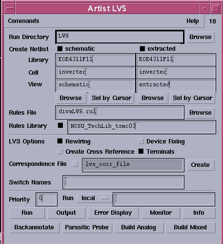
Click on the Run button and wait!!
- To
see if the job is still running, you can click on the Job Monitor... button in the LVS window
and a pop up menu will appear.
5. A pop up menu will appear notifying you of the successful completion or failure of the LVS job.

Click on the OK button.
6. Click on output from the LVS window now. A window will pop-up and you will see the following. This is the si.log output file.
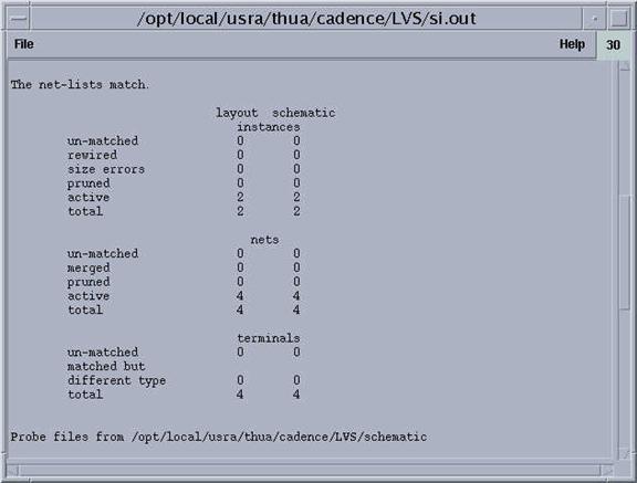
7. We see from the run log above that there are no errors in the comparison. However, there could have been error, if for example the W and L of the transistors in the schematic window did not match with the W and the L of the transistors in the layout. If your terminal names are different, it will also warn you. If you have any error, click on Error Display... in the LVS menu to view what went wrong. It is very beneficial if you click on Help in the si.log output window shown above. It will explain each of the terms in the above window in great detail.
The following points illustrate a situation if we had an error in the previous step.
8. By clicking on the Error Display, you would see the following.
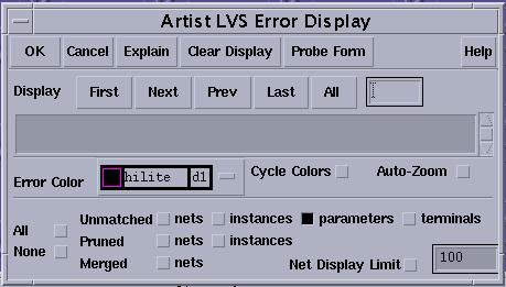
Select or deselect the various options so that the errors that will be shown are only those that you want to see at this point. In our case, the only errors we encounter is the size errors and to see that we select parameters under the Unmatched field.
10. Click
on the Display Errors button. You'll see the errors being highlighted by a
green dot in the extracted window.
11. To
get more information about the error, click on the Explain
Error button. Then move your
cursor above the highlighted point/area (in this case the bright green dot) and
click on the left mouse button. A pop up
menu will appear. Sometimes the
information given is not very helpful.
This is where your problem solving skills come to play and are being
sharpened.
12. Modify
the layout or schematic appropriately and rerun the LVS till your design is
perfectly matched.
13. There's also a feature which can help you in debugging especially checking the connection of your nets. You can access this feature by choosing Probe... from the Verify menu in your extracted view. A pop up window will appear as shown below. The following window may look a little different. It does not matter.
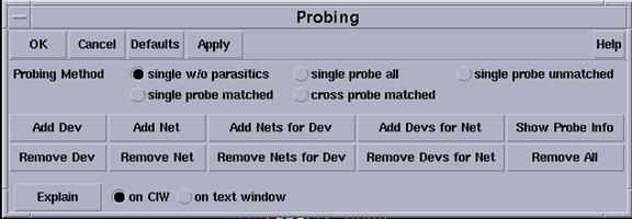
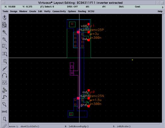
14. Click on the Add Device or Net button and then move your cursor to the net you want to be highlighted and click on the left mouse button. Anything that's connected to that net will be highlighted. An example of the highlight is shown below (note about the highlighted regions in purple):
11. Post Layout Simulation
The parasitic capacitances created according to how your layout is done at times might be critical in affecting the actual performance of your design. In order to get an idea of how the design would work from your layout, you should perform a post-layout simulation from the extracted view. The procedure is very close to that for simulating from the schematic view.
Before
simulating the extracted view, make sure that you perform the
LVS in the layout view while you have the pins "vdd!" and
"gnd!" included in the layout
(the exclamation point '!' is required to match the global vdd and
gnd from the schematic). This confirms that the logic in your layout
matches the logic in your schematic.
After
your schematic and layout match (LVS succeeds and you have no
errors), go back into your layout. Change the names of "vdd!"
and "gnd!"
to "vdd" and "gnd", respectively (just delete the
exclamation points). Save
the layout, and extract the layout (using Verify -> Extract... and setting
switches to "extract_parasitic_caps"). The following the steps below.
1. Open up your extracted view of the inverter in edit mode. To start spectre, click on Tools -->Analog Environment in the window. Two windows will pop-up. One of them is just some information window about using Analog Environment. It is possible that you may not see the information window at all. But you should see the following window. This window is the Virtuoso Analog Design Environment window.
2. Click on Setup --> Simulator/Directory/Host. Enter the fields as shown below. Choose spectre as your simulator.
3. Click on SetupàModel Path. And then select the model file tsmc25N.m and tsmc25P.m from ~/cadence/models. Then click on the button Add to make the model file active.
4. Click on Setup -> Stimuli. By default the "Inputs" stimulus type will be selected, and you should see a list of all of your input terminals in the listbox. For each item in the list, set the appropriate Function (dc or pulse) as well as the appropriate values (voltages, periods and pulse widths, etc.), select the Enabled box, and click the Change button (for each signal!). Before you click "OK" to exit the menu, look at the listbox and make sure that each line begins with ON, indicating that you have properly turned on each input signal. Now click "OK" to exit the menu.
- To select the outputs to be plotted, use Outputs -> To Be Plotted -> Select
on Schematic. After selecting this option from your menu, go to the extracted
view window and click on the wire that connects to each of the outputs that
you wish to plot (for instance, In and Out). You will have to click on the
wire, NOT just the terminal. When you are finished, you should see the list
of your outputs in the "Analog Design Environment" window. If it's too tricky
to find your output wires, you can re-extract your layout and, instead of just
setting Set Switches to "extract parasitic caps", ALSO select "include pin
names" (hold down the Control button and click on both options, then click
OK/Set Switches).
6. Click
on the second button from the top from the
set of buttons provided at the right hand side of the Virtuoso Analog Design Environment window.
This button is for Analyses. A
menu will pop-up. Enter the type of analysis as Tran
(for transient) and enter the time limits for simulation like you did
previously in schematic simulation. Try to set a reasonable time limit based on
the input you give in step 4.
7. Go to simulation menu in the Virtuoso Analog Design Environment window and click on Run. This will start simulation.
8. The CIW window should show "Reading Simulation Data ...... Successful", to ensure that simulation was a success. If not go to Simulation --> Output Log in your Virtuoso Analog Design Environment to find out what the problem was. If the simulation was successful, the waveform Window will pop up and show the input and output as shown in the figure below. The netlist for extracted view contains parasitic capacitances from various sources, including the interconnection wires. So the post-layout simulation gives more realistic results.
Note: with the extracted view, the
simulation goes pretty much the same as before. The only difference is that now
possible layout effects could be considered for a more realistic simulation.
Compared the delay from extracted
view simulation and schematic view simulation you obtained before, how much
extra delay is incurred?
Summary:
Up to now, you have basically finished a working inverter design at the design level. There are two extra steps before it can be actually sent to be manufactured so that you will get a real semiconductor chip. Additional materials on this will be posted when we come to this final step. The point here is that you need to go through the same steps for each circuit to be customarily designed in Cadence.
What to submit for HW1:
(1) please provide a hard copy of each of the following items
1. a print of your inverter circuit schematic
2. a print of your inverter test circuit schematic
3. a print of your inverter layout (showing all layers)
4. a print of the verification status of your inverter circuit passing DRC
5. a print of the extracted inverter layout
6. a print of the verification status of LVS succeeding
7. a print of the input/output waveforms showing the correct operation of inverter with the extracted inverter layout
Note: (a) if verification status information on
the window can not be saved as a .txt file, try to use snapshot in UNIX to save
it a .jpg file.
Note: for all following problems,
please set your input pulse to have a period in the order of a few nano
seconds, duty cycle of 50% and fall/rise time of 10ps.
(2) Next, make the inverter a minimum size inverter (W/L=1.5 for NMOS, L is kept at minimum 0.3u), attach a loading capacitor of 500fF, find out what should be the W/L for PMOS (L is kept at minimum) in order to have roughly equal rise and fall time (or equal low-to-high and high-to-low delay)?
(3) Set initial inverter sizes to what you find in (2) (say W/L=1.5 for NMOS, W/L=3.5 for PMOS, L=0.3um), attach a loading capacitor of 100fF to 1900fF in steps of 300fF and simulate the circuit. Measure the delay for the each case and draw a graph with load capacitance on x-axis and rise-time and fall time on y-axis. Submit the graph.
(4) Set initial inverter sizes to what you find in (2). Then attach a loading capacitor of 500fF and adjust the W/L for NMOS in steps of 0.3 while always keeping the ratio of W/L of PMOS to W/L of NMOS fixed. Measure the delay for each case and draw a graph with W/L ratio on the x-axis and rise-time and fall-time on the y-axis. Submit the graph (you can sample 6-8 points). Repeat it for a loading capacitor of 50fF.
Note:
1)
the delay depends on the input waveform you give. A
sharp transition for a pulse will always cause a smaller delay compared to a
slow transition. You have the choice to set the transition time (the rise time
and fall time for pulse), but please provide this information when you submit
it.
2)
When doing (2) to (4), you can measure the delay from schematic simulation
results. It is NOT required to use extracted layout simulation results, which
takes more effort since you have to change the layout.