
Go to the Physics Department's Home Page
Go to the Physics Department's Graduate Program Home Page
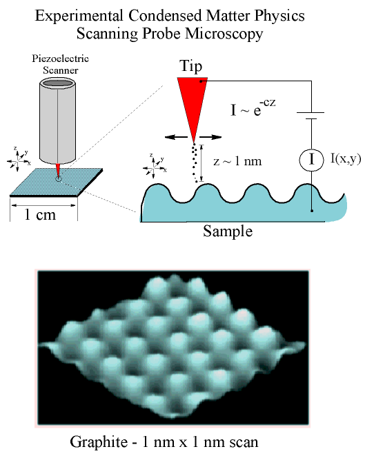
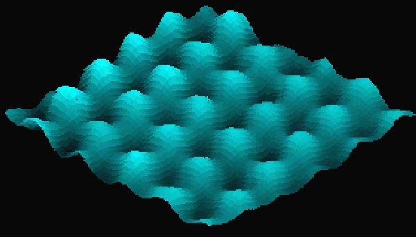
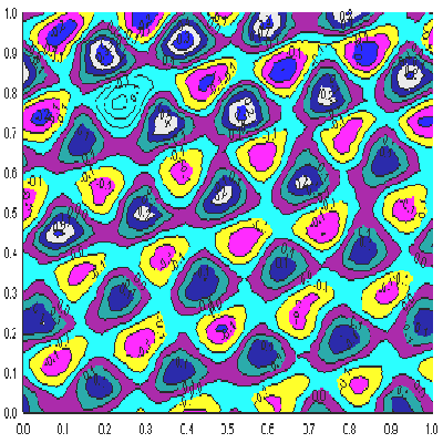
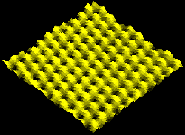
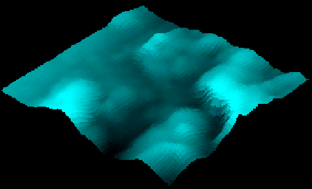
A scanning tunneling microscope (STM) provides a way to examine surfaces with atomic resolution. The STM operates by scanning a sharp probe - usually the tip of a sharpened wire - over the surface to be studied. The tip's height above the surface is controlled to be about 1 nm or less. (1 nm = 10-9m or about 40 billionths of an inch, for the metrically challenged.)
Even though the tip and sample are not touching, they can exchange electrons by quantum mechanical tunneling. A net exchange of electrons can be sustained by applying a small bias voltage between the tip and sample. This resulting tunneling current is very sensitive to changes in tip/sample separation. By rastering the tip over the surface and recording the variations in the tunneling current due to variations in the surface height, a map of the surface can be produced. Alternatively, a feedback system can raise and lower the tip to maintain a constant current as the tip is scanned. The feedback signal, applied to a piezoelectric element, then provides a measure of the surface topography. A few of these images are available here.
